Difference between revisions of "Surface Analysis (KLA/Tencor Surfscan)"
Jump to navigation
Jump to search
(reorg, remove old SOP, replaced with new PDF SOP's for each wafer size) |
|||
| Line 16: | Line 16: | ||
==Documentation== |
==Documentation== |
||
| + | === Operating Procedures === |
||
| − | *[[KLA-Tencor Surfscan - Standard Operating Procedure|Standard Operating Procedure]] |
||
| + | |||
| − | *[https://wiki.nanotech.ucsb.edu/w/images/9/96/Surfscan-Operation-Manual.pdf Operations Manual] |
||
| ⚫ | |||
| ⚫ | |||
| ⚫ | |||
| ⚫ | |||
| ⚫ | |||
| + | *[https://wiki.nanofab.ucsb.edu/w/images/4/4e/SURFSCAN_6200_Small_substrates.pdf Surfscan 6200 Small samples] * |
||
*[[Wafer scanning process traveler]] |
*[[Wafer scanning process traveler]] |
||
| + | **''This is the procedure Staff uses to calibrate particle counts on our deposition tools.'' |
||
| ⚫ | |||
| − | *[[Errors]] |
||
| + | === Other Documentation === |
||
| − | ==Standard Recipes== |
||
| − | * [https://wiki. |
+ | * [https://wiki.nanotech.ucsb.edu/w/images/9/96/Surfscan-Operation-Manual.pdf Operations Manual] |
| ⚫ | |||
| ⚫ | |||
| + | |||
| ⚫ | |||
| ⚫ | |||
| ⚫ | |||
| + | *[[Surfscan Errors and Workarounds|Common Errors & Workarounds]] |
||
| ⚫ | |||
==Examples== |
==Examples== |
||
Revision as of 11:34, 4 January 2024
| ||||||||||||||||||||||||||
About
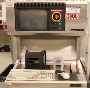
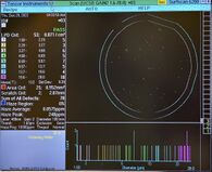
This system uses a laser-based scattering method to count size and distribution of particles (or other scattering defects) on a flat wafer surface. It can scan wafers in size from 4 to 8 inches.
Documentation
Operating Procedures
- Surfscan 6200 8inch wafers *
- Surfscan 6200 6inch wafers *
- Surfscan 6200 4inch wafers *
- Surfscan 6200 2 and 3inch wafers *
- Surfscan 6200 Small samples *
- Wafer scanning process traveler
- This is the procedure Staff uses to calibrate particle counts on our deposition tools.
Other Documentation
- Operations Manual
- For detailed measurement info, it is highly recommended that you read the manual.
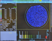
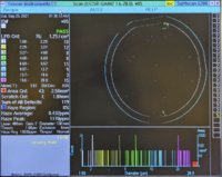
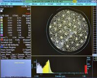
Examples
| Gain 4: Small Particles
(0.160µm – 1.60µm) |
Gain 2: Large Particles
(1.60µm – 28.0µm) |
|---|---|
|
|
| Gain 4: Small Particles
(0.160µm – 1.60µm) |
Gain 2: Large Particles
(1.60µm – 28.0µm) |
|---|---|
|
|
