Difference between revisions of "Process Group - Process Control Data"
Jump to navigation
Jump to search
(→Oxford PlasmaPro Cobra Etcher: link to new Google sheets data (ND's)) |
(increased all heading levels to get HR's between Dep/Etch sections) |
||
| Line 1: | Line 1: | ||
These are the same links found on individual tool pages, in the '''''Recipes > <<tool page>> > Process Control''''' section. |
These are the same links found on individual tool pages, in the '''''Recipes > <<tool page>> > Process Control''''' section. |
||
| − | + | =Deposition (Process Control Data)= |
|
| + | ''Process Control data for various deposition tools in the lab.'' |
||
| − | + | ==[[PECVD Recipes#PECVD 1 .28PlasmaTherm 790.29|PECVD #1 (PlasmaTherm 790)]]== |
|
*[https://docs.google.com/spreadsheets/d/1fTDNXxpf4tgNYLIEs_jvehG1KvtXqqTRDBI7sHNAVvo/edit#gid=1270764394 PECVD#1: Plots of all data] |
*[https://docs.google.com/spreadsheets/d/1fTDNXxpf4tgNYLIEs_jvehG1KvtXqqTRDBI7sHNAVvo/edit#gid=1270764394 PECVD#1: Plots of all data] |
||
| Line 9: | Line 10: | ||
*[https://docs.google.com/spreadsheets/d/1fTDNXxpf4tgNYLIEs_jvehG1KvtXqqTRDBI7sHNAVvo/edit#gid=98787450 PECVD#1: Si<sub>3</sub>N<sub>4</sub>] |
*[https://docs.google.com/spreadsheets/d/1fTDNXxpf4tgNYLIEs_jvehG1KvtXqqTRDBI7sHNAVvo/edit#gid=98787450 PECVD#1: Si<sub>3</sub>N<sub>4</sub>] |
||
| − | + | ==[[PECVD Recipes#PECVD 2 .28Advanced Vacuum.29|PECVD #2 (Advanced Vacuum)]]== |
|
*[https://docs.google.com/spreadsheets/d/1iSW1eAAg824y9PYYLG9aiaw53PEJ-f9ofylpVlCDq9Y/edit#gid=272916741 PECVD#2: Plots of all data] |
*[https://docs.google.com/spreadsheets/d/1iSW1eAAg824y9PYYLG9aiaw53PEJ-f9ofylpVlCDq9Y/edit#gid=272916741 PECVD#2: Plots of all data] |
||
| Line 17: | Line 18: | ||
**[https://docs.google.com/spreadsheets/d/1iSW1eAAg824y9PYYLG9aiaw53PEJ-f9ofylpVlCDq9Y/edit#gid=203400760 Plots of Low-Stress Si<sub>3</sub>N<sub>4</sub> Data] |
**[https://docs.google.com/spreadsheets/d/1iSW1eAAg824y9PYYLG9aiaw53PEJ-f9ofylpVlCDq9Y/edit#gid=203400760 Plots of Low-Stress Si<sub>3</sub>N<sub>4</sub> Data] |
||
| − | + | ==[[PECVD Recipes#ICP-PECVD .28Unaxis VLR.29|ICP-PECVD (Unaxis VLR Dep)]]== |
|
*[https://docs.google.com/spreadsheets/d/1CuDMKFTTzGLL6CP-FEI_9cOnUaIw-432ppDFssB59wY/edit#gid=417334948https://docs.google.com/spreadsheets/d/1CuDMKFTTzGLL6CP-FEI_9cOnUaIw-432ppDFssB59wY/edit#gid=417334948 ICP-PECVD: Plots of SiO<sub>2</sub> Films] |
*[https://docs.google.com/spreadsheets/d/1CuDMKFTTzGLL6CP-FEI_9cOnUaIw-432ppDFssB59wY/edit#gid=417334948https://docs.google.com/spreadsheets/d/1CuDMKFTTzGLL6CP-FEI_9cOnUaIw-432ppDFssB59wY/edit#gid=417334948 ICP-PECVD: Plots of SiO<sub>2</sub> Films] |
||
| Line 26: | Line 27: | ||
*[https://docs.google.com/spreadsheets/d/1CuDMKFTTzGLL6CP-FEI_9cOnUaIw-432ppDFssB59wY/edit#gid=1517031044 ICP-PECVD: Si<sub>3</sub>N<sub>4</sub> Low-Stress] |
*[https://docs.google.com/spreadsheets/d/1CuDMKFTTzGLL6CP-FEI_9cOnUaIw-432ppDFssB59wY/edit#gid=1517031044 ICP-PECVD: Si<sub>3</sub>N<sub>4</sub> Low-Stress] |
||
| − | + | ==[[Sputtering Recipes#Ion Beam Deposition .28Veeco NEXUS.29|Ion Beam Sputter Deposition (Veeco Nexus)]]== |
|
*[https://docs.google.com/spreadsheets/d/11A0ac8NU51bmcQ_grQcq9wuPwWnfy1_9MNk2DEo5yyo/edit#gid=2030038046 IBD: Plots of all data] |
*[https://docs.google.com/spreadsheets/d/11A0ac8NU51bmcQ_grQcq9wuPwWnfy1_9MNk2DEo5yyo/edit#gid=2030038046 IBD: Plots of all data] |
||
| Line 40: | Line 41: | ||
*[[Old Deposition Data - 2021-12-15]] |
*[[Old Deposition Data - 2021-12-15]] |
||
| + | |||
| ⚫ | |||
| + | <hr style="height:5px"> |
||
| ⚫ | |||
| + | <hr style="height:5px"> |
||
| ⚫ | |||
| + | ''Process Control data for various dry etching tools in the lab.'' |
||
| + | |||
| ⚫ | |||
*[https://docs.google.com/spreadsheets/d/15hYkCqL3UNNayt4sXrvVi4mBj-OSdnF7PE29mQW9AEY/edit?usp=sharing SiO<sub>2</sub> Etching with CHF3/CF4 - '''Etch Data'''] |
*[https://docs.google.com/spreadsheets/d/15hYkCqL3UNNayt4sXrvVi4mBj-OSdnF7PE29mQW9AEY/edit?usp=sharing SiO<sub>2</sub> Etching with CHF3/CF4 - '''Etch Data'''] |
||
| Line 50: | Line 56: | ||
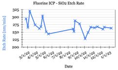
*[[Test Data of Etching SiO2 with CHF3/CF4-Fluorine ICP Etcher|SiO<sub>2</sub> Etching with CHF3/CF4 (FL-ICP]]) - ''No data prior to 2023-01-20'' |
*[[Test Data of Etching SiO2 with CHF3/CF4-Fluorine ICP Etcher|SiO<sub>2</sub> Etching with CHF3/CF4 (FL-ICP]]) - ''No data prior to 2023-01-20'' |
||
| − | + | ==[[ICP Etching Recipes#Process Control Data .28Panasonic 1.29|Panasonic ICP #1]]== |
|
*[https://docs.google.com/spreadsheets/d/1gBqCYXSl7IqpNL-yI11cuURlfZpTWwXUVM9hY_gGpT8/edit?usp=sharing SiO<sub>2</sub> Etch with CHF<sub>3</sub>/CF<sub>4</sub> - '''Etch Data'''] |
*[https://docs.google.com/spreadsheets/d/1gBqCYXSl7IqpNL-yI11cuURlfZpTWwXUVM9hY_gGpT8/edit?usp=sharing SiO<sub>2</sub> Etch with CHF<sub>3</sub>/CF<sub>4</sub> - '''Etch Data'''] |
||
| Line 59: | Line 65: | ||
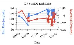
*[[Test Data of etching SiO2 with CHF3/CF4-ICP1|SiO<sub>2</sub> Etch with CHF<sub>3</sub>/CF<sub>4</sub> (Panasonic 1)]] - ''No data prior to 2023-01-20'' |
*[[Test Data of etching SiO2 with CHF3/CF4-ICP1|SiO<sub>2</sub> Etch with CHF<sub>3</sub>/CF<sub>4</sub> (Panasonic 1)]] - ''No data prior to 2023-01-20'' |
||
| − | + | ==[[ICP Etching Recipes#Process Control Data .28Panasonic 2.29|Panasonic ICP#2]]== |
|
*[https://docs.google.com/spreadsheets/d/1m0l_UK2lDxlgww4f6nfXe4aQedNeDZsLs46jQ5wR4zw/edit?usp=sharing SiO2 Etch with CHF3/CF4 - '''Etch Data'''] |
*[https://docs.google.com/spreadsheets/d/1m0l_UK2lDxlgww4f6nfXe4aQedNeDZsLs46jQ5wR4zw/edit?usp=sharing SiO2 Etch with CHF3/CF4 - '''Etch Data'''] |
||
| Line 68: | Line 74: | ||
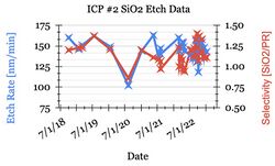
*[[Test Data of etching SiO2 with CHF3/CF4|SiO2 Etching with CHF3/CF4 - ICP2]] - ''No data prior to 2023-01-20'' |
*[[Test Data of etching SiO2 with CHF3/CF4|SiO2 Etching with CHF3/CF4 - ICP2]] - ''No data prior to 2023-01-20'' |
||
| − | + | ==[[ICP Etching Recipes#Process Control Data .28Unaxis VLR.29|Unaxis VLR Etch]]== |
|
*[[Unaxis VLR Etch - Process Control Data|InP Etching with Cl2/N2 @ 200°C - Unaxis Etch]] |
*[[Unaxis VLR Etch - Process Control Data|InP Etching with Cl2/N2 @ 200°C - Unaxis Etch]] |
||
| − | + | ==[[ICP Etching Recipes#Process Control Data .28Oxford ICP Etcher.29|Oxford PlasmaPro Cobra Etcher]]== |
|
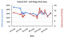
''Calibration / Process testing data taken using the "InP Ridge Etch" process: Cl2/CH4/H2 @ 60°C, 1cm piece with ~50% SiO2 hardmask.'' |
''Calibration / Process testing data taken using the "InP Ridge Etch" process: Cl2/CH4/H2 @ 60°C, 1cm piece with ~50% SiO2 hardmask.'' |
||
| − | * |
+ | *[https://docs.google.com/spreadsheets/d/1cEUB7K5BAg9N4vp3rPZw7g0orFkxeQmRkX34Fb4eZco/edit?usp=sharing "Std InP Ridge Etch" Cl<sub>2</sub>/CH<sub>4</sub>/H<sub>2</sub>/60°C - '''Etch Data Tables'''] |
| − | * |
+ | *[https://docs.google.com/spreadsheets/d/1cEUB7K5BAg9N4vp3rPZw7g0orFkxeQmRkX34Fb4eZco/edit#gid=1804752281 "Std InP Ridge Etch" Cl<sub>2</sub>/CH<sub>4</sub>/H<sub>2</sub>/60°C - '''Plots'''][[File:Oxford-ICP-Etch Process Control Data Example.jpg|alt=example SPC chart for Oxford ICP Etcher|none|thumb|225x225px|[https://docs.google.com/spreadsheets/d/1cEUB7K5BAg9N4vp3rPZw7g0orFkxeQmRkX34Fb4eZco/edit#gid=1804752281 Click for Process Control Charts]|link=https://docs.google.com/spreadsheets/d/1cEUB7K5BAg9N4vp3rPZw7g0orFkxeQmRkX34Fb4eZco/edit#gid=1804752281]] |
| − | ==== |
+ | ====Old Process Control Data==== |
*[[Oxford ICP Etcher - Process Control Data|InP Ridge Etch with Cl2/CH4/H2 @ 60°C]] - ''No data prior to 2023-01-20'' |
*[[Oxford ICP Etcher - Process Control Data|InP Ridge Etch with Cl2/CH4/H2 @ 60°C]] - ''No data prior to 2023-01-20'' |
||
Revision as of 12:56, 20 January 2023
These are the same links found on individual tool pages, in the Recipes > <<tool page>> > Process Control section.
Deposition (Process Control Data)
Process Control data for various deposition tools in the lab.
PECVD #1 (PlasmaTherm 790)
PECVD #2 (Advanced Vacuum)
ICP-PECVD (Unaxis VLR Dep)
- ICP-PECVD: Plots of SiO2 Films
- ICP-PECVD: Plots of Si3N4 Films
- ICP-PECVD: SiO2 Low-Dep Rate (LDR)
- ICP-PECVD: SiO2 High-Dep Rate (HDR)
- ICP-PECVD: Si3N4
- ICP-PECVD: Si3N4 Low-Stress
Ion Beam Sputter Deposition (Veeco Nexus)
Old Data (Pre 2022)
Old data in a different format can be found below:
Etching (Process Control Data)
Process Control data for various dry etching tools in the lab.
PlasmaTherm SLR Fluorine Etcher
OLD Process Control Data
- SiO2 Etching with CHF3/CF4 (FL-ICP) - No data prior to 2023-01-20
Panasonic ICP #1
Old Process Control Data
- SiO2 Etch with CHF3/CF4 (Panasonic 1) - No data prior to 2023-01-20
Panasonic ICP#2
Old Process Control Data
- SiO2 Etching with CHF3/CF4 - ICP2 - No data prior to 2023-01-20
Unaxis VLR Etch
Oxford PlasmaPro Cobra Etcher
Calibration / Process testing data taken using the "InP Ridge Etch" process: Cl2/CH4/H2 @ 60°C, 1cm piece with ~50% SiO2 hardmask.
- "Std InP Ridge Etch" Cl2/CH4/H2/60°C - Etch Data Tables
- "Std InP Ridge Etch" Cl2/CH4/H2/60°C - Plots
Old Process Control Data
- InP Ridge Etch with Cl2/CH4/H2 @ 60°C - No data prior to 2023-01-20