Old Deposition Data - 2021-12-15
OLD Data: Copied on 2021-12-14
From PECVD Recipes page:
Back to Vacuum Deposition Recipes.
PECVD 1 (PlasmaTherm 790)
Historical Particulate Data
- Particulates(Gain4) in PECVD#1-OLD DATA 2015
- Particulates(Gain4) in PECVD#1-OLD DATA 2016
- Particulates(Gain4) in PECVD#1-OLD DATA 2017
- Particulates in PECVD#1 films 2017
- Particulates in PECVD#1 films 2018
- Particulates in PECVD#1 films 2019
- Particulates in PECVD#1 films 2020
- Particulates in PECVD#1 films 2021
SiN deposition (PECVD #1)
Historical Data
Thin-Film Properties
- SiN 100nm Data 2014
- SiN 100nm Data 2015
- SiN 100nm Data 2016
- SiN 100nm Data 2017
- SiN 300nm Data 2017
- SiN 300nm Data 2018
- SiN 300nm Data 2019
- SiN 300nm Data 2020
- SiN 300nm Data 2021
Uniformity Data
- SiN 100 nm Thickness uniformity 2014
- SiN 100 nm Thickness uniformity 2015
- SiN 100 nm Thickness uniformity 2016
- SiN 100 nm Thickness uniformity 2017
- SiN 300nm Thickness uniformity 2017
- SiN 300nm Thickness uniformity 2018
- SiN 300nm Thickness uniformity 2019
- SiN 300nm Thickness uniformity 2020
- SiN 300nm Thickness uniformity 2021
SiO2 deposition (PECVD #1)
Historical Data
Thin-Film Properties
- SiO2 100nm Data 2014
- SiO2 100nm Data 2015
- SiO2 100nm Data 2016
- SiO2 100nm Data 2017
- SiO2 300nm Data 2017
- SiO2 300nm Data 2018
- SiO2 300nm Data 2019
- SiO2 300nm Data 2020
- SiO2 300nm Data 2021
Thick-Film Properties
Uniformity Data
- SiO2 100nm Thickness uniformity 2014
- SiO2 100 nm Thickness uniformity 2015
- SiO2 100 nmThickness uniformity 2016
- SiO2 100nm Thickness uniformity 2017
- SiO2 300nm Thickness uniformity 2017
- SiO2 300nm Thickness uniformity 2018
- SiO2 300nm Thickness uniformity 2019
- SiO2 300nm Thickness uniformity 2020
- SiO2 300nm Thickness uniformity 2021
Low-Stress SiN - LS-SiN (PECVD#1)
SiOxNy deposition (PECVD #1)
Cleaning Recipes (PECVD #1)
The cleaning procedure is very important in order to have consistent result on this tool and also to keep particulate count low. After each deposition you should clean the tool following instructions carefully. The clean is done in two steps:
- Wet cleaning (start cleaning by using a cleanroom wipe sprayed with DI. Wipe chamber sidewalls with it. Finish cleaning by using the cleanroom wipe sprayed with IPA. )
- Load the recipe for cleaning "CF4/O2 Clean" (edit the recipe and change ONLY time of cleaning). Follow instructions regarding a required time for cleaning.
Standard Cleaning Recipe: "CF4/O2 Clean"
Click the above link for a screenshot of the standard cleaning recipe, for which you will enter a custom time. The recipe is set up so that it will pop up a window for the cleaning time upon running the recipe - you do not need to edit the recipe before running it.
PECVD 2 (Advanced Vacuum)
Historical Particulate Data
- Particulates (Gain4) in PECVD#2 2015
- Particulates (Gain4) in PECVD#2 2016
- Particulates (Gain4) in PECVD#2 2017
- Particulates in PECVD#2 films 2017
- Particulates in PECVD#2 films 2018
- Particulates in PECVD#2 films 2019
- Particulates in PECVD#2 films 2020
- Particulates in PECVD#2 films 2021
SiO2 deposition (PECVD #2)
Standard Recipe
Historical Data
Thin-Film Properties
- Oxide Data 2014
- Oxide Data 2015
- Oxide data 2016
- Oxide Data 2017
- Oxide Data 2018
- Oxide Data 2019
- Oxide Data 2020
- Oxide Data 2021
Thin-Film Properties
Uniformity Data
- Oxide Thickness Uniformity 2014
- Oxide Thickness Uniformity 2015
- Oxide Thickness Uniformity 2016
- Oxide Thickness Uniformity 2017
- Oxide Thickness Uniformity 2018
- Oxide Thickness Uniformity 2019
- Oxide Thickness Uniformity 2020
- Oxide Thickness Uniformity 2021
SiN deposition (PECVD #2)
Standard Recipe
Historical Data
Thin-Film Properties
- Nitride2 Data 2014
- Nitride2 Data 2015
- Nitride2 Data 2016
- Nitride2 Data 2017
- Nitride2 Data 2018
- Nitride2 Data 2019
- Nitride2 Data 2020
- Nitride2 Data 2021
Uniformity Data
- Nitride2 Thickness Uniformity 2014
- Nitride2 Thickness Uniformity 2015
- Nitride2 Thickness Uniformity 2016
- Nitride2 Thickness Uniformity 2017
- Nitride2 Thickness Uniformity 2018
- Nitride2 Thickness Uniformity 2019
- Nitride2 Thickness Uniformity 2020
- Nitride2 Thickness Uniformity 2021
Low-Stress SiN deposition (PECVD #2)
Low-Stress SilIcon Nitride (< 100 MPa)
Standard Recipe
- STD LS Nitride2 Recipe
- Old Versions:
Historical Data
Thin-Film Properties
- LS Nitride2 Data 2014
- LS Nitride2 Data 2015
- LS Nitride2 Data 2016
- LS Nitride2 Data 2017
- LS Nitride2 Data 2018
- LS Nitride2 Data 2019
- LS Nitride2 Data 2020
- LS Nitride2 Data 2021
Uniformity Data
- LS Nitride2 Thickness Uniformity 2014
- LS Nitride2 Thickness Uniformity 2015
- LS Nitride2 Thickness Uniformity 2016
- LS Nitride2 Thickness Uniformity 2017
- LS Nitride2 Thickness Uniformity 2018
- LS Nitride2 Thickness Uniformity 2019
- LS Nitride2 Thickness Uniformity 2020
- LS Nitride2 Thickness Uniformity 2021
Amorphous-Si deposition (PECVD #2)
Cleaning Recipes (PECVD #2)
Cleaning Procedure (PECVD#2)
The cleaning procedure is very important in order to have consistent result on this tool and also to keep particulate count low. After each deposition you should clean the tool following instructions carefully. The clean is done in two steps:
- (If >29min dep time) Wet cleaning: Start cleaning by using a cleanroom wipe sprayed with DI. Wipe upper chamber sidewalls with it. Finish cleaning by using the cleanroom wipe sprayed with IPA & wiping again.
- Load the recipe for cleaning "STD CF4/O2 Clean" (edit the recipe and change ONLY time of cleaning). Follow instructions regarding required time for cleaning.
Standard Clean Recipe: "STD CF4/O2 Clean recipe"
Click the above link for a screenshot of the standard cleaning recipe, for which you will enter a custom time. The recipe is set up so that it will pop up a window for the cleaning time upon running the recipe - you do not need to edit the recipe before running it.
Clean Times (PECVD#2)
| Film Deposited | Cleaning Time (Dry) |
|---|---|
| SiO2 | 1 min. clean for every 1 min. deposition |
| Si3N4 | 1 min. clean for every 7 min of deposition |
| If > 29min total dep time
(Season + Dep) |
Wet Clean the Upper Lid/Chamber
DI water then Isopropyl Alcohol on chamber wall & portholes |
ICP-PECVD (Unaxis VLR)
2020-02: New recipes have been characterized for low particulate count and repeatability. Only staff-supplied recipes are allowed in the tool. Please follow the new procedures to ensure low particle counts in the chamber.
The system currently has Deuterated Silane (SiD4) installed - identical to the regular Silicon precursor SiH4, except that it significantly lowers optical absorption in the near-infrared due to shifted molecular vibrations/molecular weights.
Historical Particulate Data
Standard Recipes
SiO2 LDR 250C Deposition (Unaxis VLR)
Low-Deposition Rate SiO2
Historical Data
Thin-Film Properties
This data is for 780sec long SiO2 LDR (low deposition rate) deposition, and cleaning time is 900sec, following the procedure here.
Uniformity Data
SiO2 HDR 250C Deposition (Unaxis VLR)
High-Deposition Rate SiO2
Historical Data
Thin-Film Properties
This data is for 180sec long SiO2 HDR ( high deposition rate) deposition, and cleaning time is 900sec, following the procedure here.
Uniformity Data
SiN 250C deposition (Unaxis VLR)
Historical Data
Thin-Film Properties
This data is for 480sec long SiN deposition, and cleaning time is 1500sec, following the procedure here.
Uniformity Data
SiN LS 250C Deposition (Unaxis VLR)
Low Stress Silicon-Nitride
Historical Data
To Be Added
Thin-Film Properties
This data is for 180sec long SiN LS (low stress) deposition, and cleaning time is 1500sec, following the procedure here.
Uniformity Data
Cleaning Recipes (Unaxis VLR Dep)
You must edit the Post-Dep Clean recipe to correspond to your deposited thickness and material. See the Operating Procedure on the Unaxis Tool Page for details.
- SiNx etches at 20nm/min
- SiO2 etches at 40nm/min
––––––––––––––––––––––––––––––––––––––––––
––––––––––––––––––––––––––––––––––––––––––
From Sputtering Recipes page:
Ion Beam Deposition (Veeco NEXUS)
- IBD Calibrations Spreadsheet - Records of historical film depositions (rates, indices), Uniformity etc.
- Users may to enter their calibration deps (simple test deps only)
SiO2 deposition (IBD)
SiO2 Historical Data
- SiO2 Standard Recipe
- SiO2 Data December 2014
- SiO2 Thickness uniformity 2014
- SiO2 Data-15min depositions 2015
- SiO2 Thickness uniformity-15 min depositions 2015
- SiO2 Data-1hr depositions 2015
- SiO2 Thickness uniformity-1hr depositions 2015
- SiO2 Data-1hr depositions 2016
- SiO2 Thickness uniformity-1hr depositions 2016
SiO2 1hr deposition properties:
- Dep.rate: ≈ 5.2 nm/min (users must calibrate this prior to critical deps)
- HF e.r.~350 nm/min
- Stress ≈ -390MPa (compressive)
- Refractive Index: ≈ 1.494
- [Cauchy Parameters] (350-2000nm):
- A = 1.480
- B = 0.00498
- C = -3.2606e-5
Si3N4 deposition (IBD)
- Deposition Rate: ≈ 4.10 nm/min (users must calibrate this prior to critical deps)
- HF e.r.~11nm/min
- Stress ≈ -1590MPa (compressive)
- Refractive Index: ≈ 1.969
- [Cauchy Parameters] (350-2000nm):
- A = 2.000
- B = 0.01974
- C = 1.2478e-4
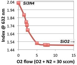
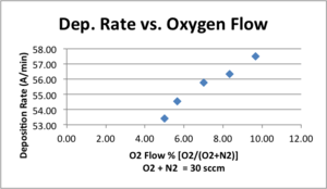
SiOxNy deposition (IBD)
These are some old (2010), initial characterizations only. A recipe improvement would be to increase the Assist O2+N2 = 60sccm total, increasing repeatability. Contact Demis for more info.
Ta2O5 deposition (IBD)
Ta2O5 Historical Data (IBD)
- Ta2O5 Data December-15 min depositions 2015
- Ta2O5 Thickness uniformity-15 min depositions 2015
- Ta2O5 Data December-1hr depositions 2015
- Ta2O5 Thickness uniformity-1hr depositions 2015
- Ta2O5 Data December-1hr depositions 2016
- Ta2O5 Thickness uniformity-1hr depositions 2016
Ta2O5 Deposition/Film Properies (IBD)
- Ta2O5 1hr depositions:
- Deposition Rate: ≈ 7.8 nm/min (users must calibrate this prior to critical deps)
- HF e.r.~2 nm/min
- Stress ≈ -232MPa (compressive)
- Refractive Index: ≈ 2.172
- [Cauchy Parameters] (350-2000nm):
- A = 2.1123
- B = 0.018901
- C = -0.016222
TiO2 deposition (IBD)
- Deposition Rate: ≈ 1.29 nm/min (users must calibrate this prior to critical deps)
- HF etch rate ~5.34nm/min
- Stress ≈ -445MPa (compressive)
- Refractive Index: ≈ 2.259
- [Cauchy Parameters] (350-2000nm):
- A = 2.435
- B = -4.9045e-4
- C = 0.01309
- Absorbing < ~350nm
Al2O3 deposition (IBD)
- Al2O3 standard recipe: 1_Al2O3_dep
- Deposition Rate: ≈ 2.05nm/min (users must calibrate this prior to critical deps)
- HF etch rate ~167nm/min
- Stress ≈ -332MPa (compressive)
- Refractive Index: ≈ 1.656
- [Cauchy Parameters] (350-2000nm):( working on)
- A =
- B =
- C =
- Absorbing < ~350nm

