Difference between revisions of "Process Group - Process Control Data"
Jump to navigation
Jump to search
(description of process control data) |
(Moved litho to the bottom since it's updated less often) |
||
| (One intermediate revision by the same user not shown) | |||
| Line 1: | Line 1: | ||
| − | Process Control Data are standardized process, run by staff, allowing for day-to-day or year-by-year comparisons of a tool's performance. |
+ | Process Control Data are standardized process, run by staff, allowing for day-to-day or year-by-year comparisons of a tool's performance. This is similar (but not identical to) [https://en.wikipedia.org/wiki/Statistical_process_control Statistical Process Control]. |
These are the same links found on individual tool pages, in the '''''Recipes > <<tool page>> > Process Control''''' section. |
These are the same links found on individual tool pages, in the '''''Recipes > <<tool page>> > Process Control''''' section. |
||
| + | __TOC__ |
||
| ⚫ | |||
| ⚫ | |||
| ⚫ | |||
| − | |||
| ⚫ | |||
| ⚫ | |||
| ⚫ | |||
| − | |||
| ⚫ | |||
| ⚫ | |[[File:ASML CD Cals - Example Table.jpg|alt=ASML CD Calibration data - Screenshot of Table|none|thumb|300x300px|''Example of Data Table with SEM's of 320nm features. [https://docs.google.com/spreadsheets/d/1xW1TFH_QjPMWl9T1jiKzwmYe4B2wg7KY-nqOKUoXttI/edit#gid=0 Click for full data table.]''|link=https://docs.google.com/spreadsheets/d/1xW1TFH_QjPMWl9T1jiKzwmYe4B2wg7KY-nqOKUoXttI/edit#gid=0]] |
||
| ⚫ | |[[File:ASML CD Cals - Example Plot.jpg|alt=ASML CD Calibration Data - Screenshot of SPC Plot|none|thumb|''Example SPC Chart - Measured Critical Dimension "CD" versus Date. [https://docs.google.com/spreadsheets/d/1xW1TFH_QjPMWl9T1jiKzwmYe4B2wg7KY-nqOKUoXttI/edit#gid=1804752281 Click for charts.]''|link=https://docs.google.com/spreadsheets/d/1xW1TFH_QjPMWl9T1jiKzwmYe4B2wg7KY-nqOKUoXttI/edit#gid=1804752281]] |
||
| ⚫ | |||
| − | |||
| ⚫ | |||
| ⚫ | |||
=Deposition (Process Control Data)= |
=Deposition (Process Control Data)= |
||
| Line 106: | Line 92: | ||
*[[Oxford ICP Etcher - Process Control Data|InP Ridge Etch with Cl2/CH4/H2 @ 60°C]] - ''No data prior to 2023-01-20'' |
*[[Oxford ICP Etcher - Process Control Data|InP Ridge Etch with Cl2/CH4/H2 @ 60°C]] - ''No data prior to 2023-01-20'' |
||
| + | |||
| + | |||
| ⚫ | |||
| ⚫ | |||
| + | |||
| ⚫ | |||
| ⚫ | |||
| + | |||
| ⚫ | |||
| + | |||
| ⚫ | |||
| ⚫ | |||
| ⚫ | |||
| + | |||
| ⚫ | |||
| ⚫ | |[[File:ASML CD Cals - Example Table.jpg|alt=ASML CD Calibration data - Screenshot of Table|none|thumb|300x300px|''Example of Data Table with SEM's of 320nm features. [https://docs.google.com/spreadsheets/d/1xW1TFH_QjPMWl9T1jiKzwmYe4B2wg7KY-nqOKUoXttI/edit#gid=0 Click for full data table.]''|link=https://docs.google.com/spreadsheets/d/1xW1TFH_QjPMWl9T1jiKzwmYe4B2wg7KY-nqOKUoXttI/edit#gid=0]] |
||
| ⚫ | |[[File:ASML CD Cals - Example Plot.jpg|alt=ASML CD Calibration Data - Screenshot of SPC Plot|none|thumb|''Example SPC Chart - Measured Critical Dimension "CD" versus Date. [https://docs.google.com/spreadsheets/d/1xW1TFH_QjPMWl9T1jiKzwmYe4B2wg7KY-nqOKUoXttI/edit#gid=1804752281 Click for charts.]''|link=https://docs.google.com/spreadsheets/d/1xW1TFH_QjPMWl9T1jiKzwmYe4B2wg7KY-nqOKUoXttI/edit#gid=1804752281]] |
||
| ⚫ | |||
Latest revision as of 12:03, 24 April 2024
Process Control Data are standardized process, run by staff, allowing for day-to-day or year-by-year comparisons of a tool's performance. This is similar (but not identical to) Statistical Process Control.
These are the same links found on individual tool pages, in the Recipes > <<tool page>> > Process Control section.
Deposition (Process Control Data)
Process Control data for various deposition tools in the lab.
PECVD #1 (PlasmaTherm 790)
PECVD #2 (Advanced Vacuum)
ICP-PECVD (Unaxis VLR Dep)
- ICP-PECVD: Plots of SiO2 Films
- ICP-PECVD: Plots of Si3N4 Films
- ICP-PECVD: SiO2 Low-Dep Rate (LDR)
- ICP-PECVD: SiO2 High-Dep Rate (HDR)
- ICP-PECVD: Si3N4
- ICP-PECVD: Si3N4 Low-Stress
Ion Beam Sputter Deposition (Veeco Nexus)
Old Data (Pre 2022)
Old data in a different format can be found below:
Etching (Process Control Data)
Process Control data for various dry etching tools in the lab.
PlasmaTherm SLR Fluorine Etcher
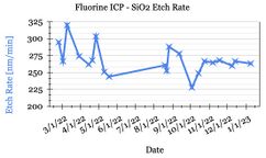
OLD Process Control Data
- SiO2 Etching with CHF3/CF4 (FL-ICP) - No data prior to 2023-01-20
Panasonic ICP #1
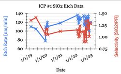
Old Process Control Data
- SiO2 Etch with CHF3/CF4 (Panasonic 1) - No data prior to 2023-01-20
Panasonic ICP#2
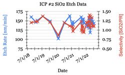
Old Process Control Data
- SiO2 Etching with CHF3/CF4 - ICP2 - No data prior to 2023-01-20
Unaxis VLR Etch
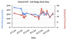
Oxford PlasmaPro Cobra Etcher
Calibration / Process testing data taken using the "InP Ridge Etch" process: Cl2/CH4/H2 @ 60°C, 1cm piece with ~50% SiO2 hardmask.
- "Std InP Ridge Etch" Cl2/CH4/H2/60°C - Etch Data Tables
- "Std InP Ridge Etch" Cl2/CH4/H2/60°C - Plots
Old Process Control Data
- InP Ridge Etch with Cl2/CH4/H2 @ 60°C - No data prior to 2023-01-20
Lithography (Process Control Data)
Process Control Data for Nanofab Lithography/patterning tools.
Stepper #3 (ASML DUV)
- The Process Group regularly measures data on lithography Critical Dimension ("CD") and Wafer-stage Particulate Contamination for this tool, using a sensitive lithography process that will reveal small changes in Dose repeatability and wafer flatness.
- Plots of CD Repeatability
- Data for CD Uniformity and Particulate Contamination
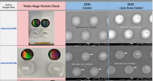 Example of Data Table with SEM's of 320nm features. Click for full data table.
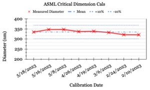 Example SPC Chart - Measured Critical Dimension "CD" versus Date. Click for charts.