Search results
Jump to navigation
Jump to search
Page title matches
- All Images3 members (1 subcategory, 2 files) - 14:14, 9 February 2017
- All images of tools. [[Category:Images]]81 members (0 subcategories, 81 files) - 08:27, 27 June 2012
Page text matches
- All images of tools. [[Category:Images]]81 members (0 subcategories, 81 files) - 08:27, 27 June 2012
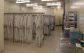
File:GowningRoom.jpg [[category:images]](4,416 × 2,800 (1.82 MB)) - 10:56, 11 July 2012
File:UnderConstruction.jpg [[category:images]](297 × 260 (22 KB)) - 08:28, 27 June 2012- <includeonly>[[Category:Tool Images]]</includeonly>51 bytes (5 words) - 15:34, 27 June 2012
- All Images3 members (1 subcategory, 2 files) - 14:14, 9 February 2017
File:CAD Tutorial for ASML Reticle v1 - screenshot Reticle Layout cell.png Example of a Reticle with 4 Images on it. The Outlines layer should not be printed.(1,700 × 1,008 (137 KB)) - 17:07, 8 December 2020- *[//wiki.nanotech.ucsb.edu/w/images/f/f5/11-CZT_etching-1.pdf CdZnTe Etch Recipes - CH<sub>4</sub>-H<sub>2</sub *[//wiki.nanotech.ucsb.edu/w/images/b/b4/ZnS_Plasma_Etch-1.pdf ZnS Etch Recipe - CH<sub>4</sub>-H<sub>2</sub>-A2 KB (253 words) - 10:02, 14 June 2021
- |SEM Images |[https://wiki.nanotech.ucsb.edu/w/images/0/0b/FE210206.pdf]322 bytes (44 words) - 18:30, 2 February 2021
- |SEM Images |[https://wiki.nanotech.ucsb.edu/w/images/0/0b/FE210206.pdf]322 bytes (44 words) - 18:37, 2 February 2021
- |SEM Images264 bytes (34 words) - 18:33, 2 February 2021
- ==Spectra Images== *[https://wiki.nanofab.ucsb.edu/w/images/8/89/DUV_Flood_Expose_SOP_Rev_C.pdf DUV Flood Expose Standard Operating Pro1 KB (207 words) - 15:40, 4 January 2024
- |SEM Images |[https://wiki.nanotech.ucsb.edu/wiki/images/f/f1/SiO2_Etch_using_ICP2_with_O2.pdf]707 bytes (100 words) - 18:26, 6 April 2020
- | colspan="4" |[https://wiki.nanotech.ucsb.edu/w/images/4/45/IP210201.pdf 1.4] mT, 125/800W, Cl2/H2/Ar flow-rate=6.3/12.7/2 sccm, |[https://wiki.nanotech.ucsb.edu/wiki/images/9/9b/IP161332.pdf]4 KB (459 words) - 18:00, 8 November 2021
- |'''SEM Images''' ...is_111822_002.jpg <nowiki>[30D]</nowiki>][https://wiki.nanotech.ucsb.edu/w/images/c/cd/CS_unaxis_111822_003.jpg <nowiki>[CS]</nowiki>]5 KB (717 words) - 18:41, 21 November 2022
- ...s UCSB NanoFab users to make calibrated measurements on microscope and SEM images with freely available software, after the image acquisition. == SEM Images ==5 KB (689 words) - 11:02, 10 June 2019
- *[//wiki.nanotech.ucsb.edu/w/images/7/7b/Xactic-XetchX3-System-Manual.pdf System Manual] *[//wiki.nanotech.ucsb.edu/w/images/c/c0/XeF2-Results.pdf Si Etching Profile & Results]2 KB (323 words) - 15:03, 30 October 2023
- |'''SEM Images''' ...n1_011123_002.jpg <nowiki>[30D]</nowiki>][https://wiki.nanotech.ucsb.edu/w/images/5/52/Cs_pan1_011123_002.jpg <nowiki>[CS]</nowiki>]7 KB (936 words) - 09:54, 12 January 2023
- *[//wiki.nanotech.ucsb.edu/w/images/b/b3/Thermal_Evaporator2.pdf Operating Instructions]963 bytes (123 words) - 10:29, 30 August 2022
- *[https://wiki.nanofab.ucsb.edu/w/images/3/3e/UV_Ozone_SOP_Rev_A.pdf UV Ozone Reactor SOP] *[//wiki.nanotech.ucsb.edu/wiki/images/7/79/UV_Ozone_Manual_Jelight_M-144AX.pdf UV Ozone Manual]961 bytes (145 words) - 09:17, 29 August 2023
- #Submit a Detailed [//wiki.nanotech.ucsb.edu/w/images/7/79/Nanofabrication_Facility_Project_Description.xlsx project description #[//wiki.nanotech.ucsb.edu/w/images/a/a2/UCSB-Facilities-Use-Agreement.pdf UCSB Facility Use Agreement (downloa10 KB (1,453 words) - 21:55, 9 January 2024


