Gallery of new files
Jump to navigation
Jump to search
This special page shows the last uploaded files.


- Holography Process for 1D-lines and 2D-dots (ARC-11 & THMR-IP3600HP-D)-updated-8-13-2018-A.pdf Ningcao
16:15, 11 October 2018
; 243 KB
 Editing Tutorial - Hyperlink panel nonexisting page 02 - CLICK arrow.png.png John d
17:00, 4 September 2018
800 × 417; 96 KB
 Click on "Create" Tab to enter VisualEditing Mode.png John d
16:53, 4 September 2018
661 × 98; 21 KB

 Editing Tutorial - Hyperlink panel nonexisting page 01.png John d
08:42, 31 August 2018
932 × 486; 60 KB

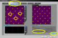
 Resolution chart OPC - Screen Shot 2018-07-23 at 1.40.48 PM.png John d
03:17, 1 August 2018
673 × 416; 26 KB
 Resolution Chart - Screen Shot 2018-07-23 at 1.36.31 PM.png John d
03:14, 1 August 2018
548 × 333; 31 KB
 GlobalMulti NEG - Screen Shot 2018-07-23 at 11.22.19 AM.png John d
02:57, 1 August 2018
115 × 113; 4 KB
 GlobalMulti POS - Screen Shot 2018-07-23 at 11.17.23 AM.png John d
02:54, 1 August 2018
145 × 145; 2 KB
 Stepper align - Screen Shot 2018-07-23 at 11.24.31 AM.png John d
02:52, 1 August 2018
292 × 122; 6 KB
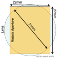
 UCSB Dicing Guides - Image Location on Reticle - 800px.png John d
02:26, 1 August 2018
800 × 600; 732 KB


 Olympus LEXT - Saturation Highlighting button highlighted.png John d
18:02, 25 July 2018
54 × 271; 20 KB
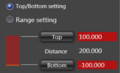
 Olympus LEXT - 3-point Leveling Screen highlighted.png John d
17:54, 25 July 2018
1,072 × 705; 345 KB
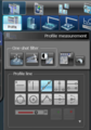


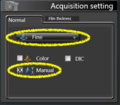 Olympus LEXT - acquisition settings - Fine, manual annot.png John d
17:23, 25 July 2018
264 × 231; 38 KB


 CDE ResMap Quarter Wafer meas location - 800px annot quarterwf.png John d
12:59, 17 April 2018
579 × 564; 510 KB
 CDE ResMap Full Wafer meas location - IMG 0112 - 800px annot.png John d
12:57, 17 April 2018
579 × 564; 500 KB
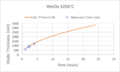
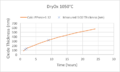
 TyStar Thermal Oxidations - WetOx 1050°C 2018-04-09 zoom.png John d
12:13, 9 April 2018
752 × 452; 36 KB
 ASML Stepper 3 - Field Sizes - Screen Shot 2018-02-21 at 1.40.22 PM.png John d
14:58, 21 February 2018
481 × 490; 45 KB
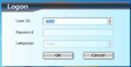
 Wiki- Log In - Screen Shot 2017-11-30 at 4.14.49 PM.png John d
17:43, 30 November 2017
287 × 65; 12 KB
 SignupMonkey - Add to Calendar - Screen Shot 2017-11-30 at 3.55.11 PM.png John d
17:22, 30 November 2017
400 × 242; 71 KB
 SignupMonkey - Add to Calendar - Screen Shot 2017-11-30 at 3.55.10 PM.png John d
17:19, 30 November 2017
300 × 182; 45 KB
- New AdvPECVD-LS Nitride2 300C standard recipe LS Nitride2 standard recipe.pdf Biljana
08:52, 20 October 2017
; 380 KB
- AdvPECVD-LS Nitride2 300C standard recipe LS Nitride2 standard recipe.pdf Biljana
08:43, 20 October 2017
; 380 KB


- Amorphous Silicon Film Deposition using 12.5W bias on SiO2-Si.pdf Ningcao
14:11, 28 July 2016
; 943 KB
- 45-Etching Nickel with Al2O3 Mask using Oxford Ion Mill Tool.pdf Ningcao
16:23, 1 December 2015
; 1.87 MB
- 44-Etching Gold with Al2O3 Mask using Oxford Ion Mill Tool.pdf Ningcao
15:49, 9 October 2015
; 2.28 MB
- Pages from FEI - Scanning Electrong Microscope - Operating Manual PART 3.pdf Hopkins a
11:32, 3 August 2015
; 3.02 MB
- Pages from FEI - Scanning Electrong Microscope - Operating Manual PART 2.pdf Hopkins a
11:32, 3 August 2015
; 3.91 MB
- Pages from FEI - Scanning Electrong Microscope - Operating Manual PART 1.pdf Hopkins a
11:32, 3 August 2015
; 3.22 MB
- 39-Medium-stress SiNx at 100C using Unaxis ICP deposition tool.pdf Ningcao
12:07, 30 June 2015
; 48 KB
- 38-High-stress SiNx at 100 C using Unaxis ICP deposition tool.pdf Ningcao
11:55, 30 June 2015
; 43 KB
- 37-Low-stress SiNx at 100 C using Unaxis ICP deposition tool.pdf Ningcao
11:39, 30 June 2015
; 169 KB
- 34-High-stress SiNx at 250 C using Unaxis ICP deposition tool.pdf Ningcao
15:59, 29 June 2015
; 10 KB
- 35-Low-stress SiNx at 250 C using Unaxis ICP deposition tool.pdf Ningcao
15:27, 29 June 2015
; 118 KB
- New Adv PECVD-LS Nitride2 300C standard recipe LS Nitride2 standard recipe.pdf Biljana
11:57, 9 January 2015
; 378 KB
- New Adv PECVD-Nitride2 300C standard recipe Nitride2 Standard Recipe.pdf Biljana
11:56, 9 January 2015
; 373 KB
- New Adv PECVD OXIDE 300C standard recipe OXIDE Standard Recipe.pdf Biljana
11:54, 9 January 2015
; 653 KB
- New PECVD1-SiO2-standard recipe 2014 SiO2 standard recipe.pdf Biljana
15:03, 8 January 2015
; 594 KB
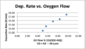
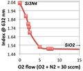
- SiN-AJA-1-Reactive-Sputtering-Power-Flow-AFM-Rate-Index-rev1.pdf Thibeault
12:41, 23 December 2014
; 336 KB
- SiO2-AJA-1-Reactive-Sputter-Power-Flow-AFM-Roughness-rev1.pdf Thibeault
12:00, 23 December 2014
; 518 KB
- 31-Holography Process for 1D-lines and 2D-dots-rev-3-13-2014.pdf Ningcao
14:22, 18 April 2014
; 624 KB
- 30-Redicing Nanowire Diameter by Thermal Oxidation and Vapored HF Etch.pdf Ningcao
14:11, 18 April 2014
; 1.31 MB


