Difference between revisions of "Resistivity Mapper (CDE RESMAP)"
Jump to navigation
Jump to search
Millerski w (talk | contribs) (Updated SOP) |
|||
| (One intermediate revision by the same user not shown) | |||
| Line 19: | Line 19: | ||
*[[CDE ResMap Quick-Start instructions]] |
*[[CDE ResMap Quick-Start instructions]] |
||
| + | *[https://wiki.nanofab.ucsb.edu/w/images/3/37/CDE_ResMap_Operating_Instructions.pdf CDE ResMap Operating Instructions] |
||
*System can export CSV files - contact supervisor for instructions. |
*System can export CSV files - contact supervisor for instructions. |
||
Latest revision as of 15:07, 30 October 2023
| ||||||||||||||||||||||||||
About
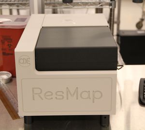
The CDE Resmap 4 point resistivity mapper is used for measuring resistivity across the wafer for substrates and thin films deposited in the facility. The system can do automated resistivity mapping for pieces to 8 inch wafers.
The resistivity range is 2 mOhm/Square to 5 MOhm/square. Contour plots, 3D plots, histograms, data exporting are supported from the Windows XP based control system.
Instructions
- CDE ResMap Quick-Start instructions
- CDE ResMap Operating Instructions
- System can export CSV files - contact supervisor for instructions.
