Difference between revisions of "Field Emission SEM 2 (JEOL IT800SHL)"
Jump to navigation
Jump to search
(copied page from SEM1, linked to SEM1 page.) |
m |
||
| (2 intermediate revisions by one other user not shown) | |||
| Line 15: | Line 15: | ||
Identical to [https://wiki.nanofab.ucsb.edu/wiki/SEM_1_(JEOL_IT800SHL) SEM#1], but with EDAX module added. |
Identical to [https://wiki.nanofab.ucsb.edu/wiki/SEM_1_(JEOL_IT800SHL) SEM#1], but with EDAX module added. |
||
| − | Please see the [https://wiki.nanofab.ucsb.edu/wiki/SEM_1_(JEOL_IT800SHL) SEM#1 page] for main tool details. |
+ | '''Please see the [https://wiki.nanofab.ucsb.edu/wiki/SEM_1_(JEOL_IT800SHL) SEM#1 page] for main tool details & procedures.''' |
| − | == |
+ | ==EDS Elemental Analysis== |
| + | |||
| − | '''Information to be added''' |
||
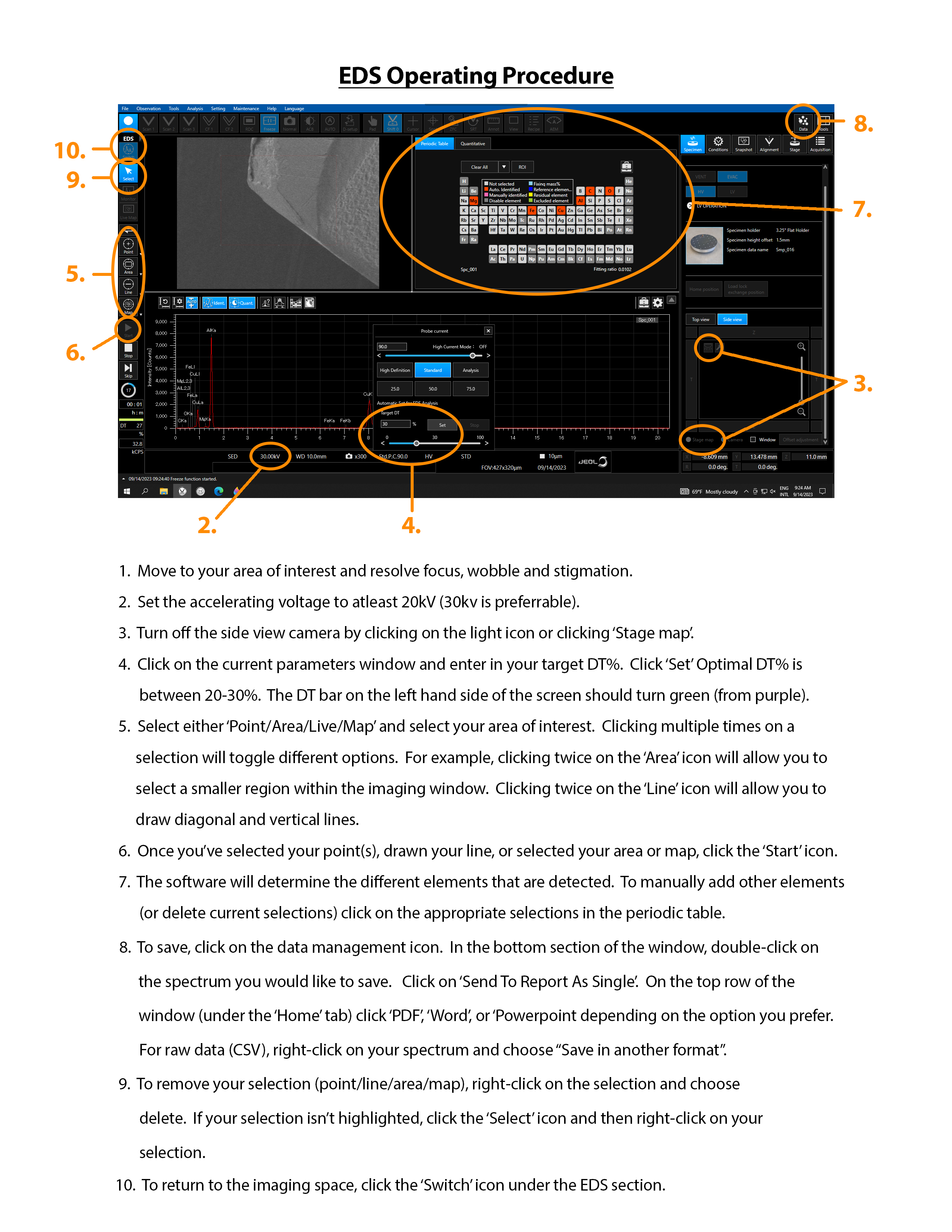
| + | *[https://wiki.nanofab.ucsb.edu/w/images/3/3a/EDS_SOP.jpg EDS Operating Procedure] |
||
Latest revision as of 21:08, 29 February 2024
| ||||||||||||||||||||||||||||||

About
The JEOL IT800HSL Field Emission Scanning Electron Microscope is used for imaging a variety of samples made in the facility.
Identical to SEM#1, but with EDAX module added.
Please see the SEM#1 page for main tool details & procedures.