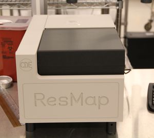
Resistivity Mapper (CDE RESMAP)
Jump to navigation
Jump to search
The printable version is no longer supported and may have rendering errors. Please update your browser bookmarks and please use the default browser print function instead.
|
About
The CDE Resmap 4 point resistivity mapper is used for measuring resistivity across the wafer for substrates and thin films deposited in the facility. The system can do automated resistivity mapping for pieces to 8 inch wafers.
The resistivity range is 2 mOhm/Square to 5 MOhm/square. Contour plots, 3D plots, histograms, data exporting are supported from the Windows XP based control system.
