Main Page

From UCSB Nanofab Wiki
Revision as of 21:37, 21 March 2019 by John d (talk | contribs) (test numbered headings)
Jump to navigation Jump to search


Welcome to the UCSB Nanofab Wiki
Arrowleft3.png See sidebar for
             Equipment & Recipes
Make sure you know the
Lab Rules
1 Stepper #3 (ASML DUV) - PM Moved to 5/6 – 5/10

We are postponing the Maintenance date to May 6th – 10th. On the week of May 6th, ASML Engineers will be performing preventative maintenance, please plan your work around the tool being down at that time.

//Vraj Mehalana 09:42, 5 April 2024 (PDT)

2 ALD Oxford UP

The tool is working properly at this time and is now available for use. Thank you for your patience in regard to this matter. //Vraj Mehalana 13:48, 19 March 2024 (PDT)

3 DI and Waste Water systems

DI and Waste Water systems will be down for upgrade April 5th and 6th. //Vraj Mehalana 11:55, 18 March 2024 (PDT)

4 ICP1 Down

The board we were waiting on arrived, but it did not resolve the tool issue. We are working with Panasonic on the next steps. //Vraj Mehalana 14:17, 1 March 2024 (PST)

5 Job Opening: Process Engineer

The Nanofab has a current job opening for a Process/Wafer-Fab Engineer, see the NanoFab Job Openings page for details.

//Demis D. John 14:52, 30 October 2023 (PDT)

6 Lab Access Changes: Symmetry App

Card/Iris scanner access is still currently enabled. However we will be moving to a smartphone-based access system. IMPORTANT: check your email to setup the new smartphone access system, so you will be ready when we switch to the new system. Look for an email titled "Invitation to Access Symmetry App". // John d 13:49, 7 November 2023 (PST)

7 Wafer Bonder, (Suss SB6-8E)

SUSS aims to be on site in early February. We’ll will send out an email once I get confirmation for a specific date. //Vraj Mehalana 14:23, 13 December 2023 (PST)

8 How to use this wiki

  • NanoFab Users are responsible for understanding their chemistry, risks and usage of various chemicals. Please read the MSDS sheets for the chemicals you use!
  • Users can add qualified processing data to the Wiki pages; see the Editing_Tutorials for how to do that.
Bay3 v1.jpg
GowningRoom v2.jpg

  • Supervisors of individuals using the facility, e.g., UCSB Principal Investigators and external user managers are ultimately responsible for ensuring that their supervisees have the appropriate knowledge and training to work safely in the facility.
  • They are also responsible for ensuring that all applicable regulatory requirements are met. This includes having a compliant "Chemical Hygiene Plan" per OSHA regulations.
  • The information on this site should be considered as providing "general supporting information" to the Chemical Hygiene Plan of a particular supervisor. Supervisors can reference all or some of this site information within their Plans. UCSB EH&S can provide assistance to supervisors in preparing their Plans.


9 News & Announcements

News from the U.C. Santa Barbara Nanofabrication Facility.

NanoFab staff awarded Goleta's Innovator of the Year 2023

NanoFab staff member Demis D. John has been awarded the City of Goleta's "Innovator of the Year" for 2023! The award stems from the UCSB Nanofab's impact on the communities of Santa Barbara County and surrounding regions, in enabling cutting edge technology companies to thrive, which also enables many local careers in advanced high-tech. See the full announcement by the Santa Barbara South Coast Chamber of Commerce. //John d 13:58, 7 November 2023 (PST)

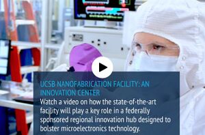
10 NanoFab Featured in Regional Tech Videos

The UCSB NanoFab is showcased as a driver of innovation and enabler of the regional high-tech industry.

See the videos here:

Santa Barbara County: This is TechTopia
Techtopia Vid - Thumbnail PlayButton.jpg
UCSB NanoFab: An Innovation Center
NanoFab COE Engineering Vid - thumbnail 2 crop.jpg

// John d 09:26, 1 November 2023 (PST)

11 CHIPS Act Award Announced to USC and UCSB NanoFab

U.S. Congressman Salud Carbajal congratulates UCSB and the NanoFab on receiving a CHIPS & Science Act award, as part of the California DREAMS Hub (Microelectronics Commons) led by USC. // Demis 12:06, 4 October 2023 (PDT)

12 JEOL SEM's Installed

Both SEM's have been replaced with new JEOL SEM's #1 and SEM #2. SEM#1 has the NABITY lithography system installed, and SEM #2 has always-on EDAX elemental analysis. Contact the supervisor, Aidan Hopkins, for more information. // John d 18:31, 20 September 2023 (PDT)

13 Wide FOV Microscope Installed

We have installed an AmScope stereo microscope in Bay 4 for wide field-of-view digital imaging/capture, with >2cm of FOV currently available. Wiki page here: AmScope Wide Field of View Stereoscope // John d 14:52, 19 April 2023 (PDT)

14 Loomis Scribe & Break installed

We have installed a new Loomis LSD-155LT Automated Scribe & Break Cleaving tool in the Back-End Processing lab. Qualifications are underway. Contact supervisor, Aidan Hopkins, for more information. // John d 09:41, 16 April 2023 (PDT)

15 Dektak XT installed

We have replaced the old Dektak 6M with a new Dektak XT profilometer. This tool will provide robust, fast metrology for rapid in-process topography inspection. // John d 10:41, 25 January 2023 (PST)

16 New Process Control data tables

We have added "Process Control Data" - data on deposition/etch repeatability - to a number of our highest used etchers and deposition tools. The datasheets are linked in multiple places, mainly on the Recipes pages for each tool, or on the general Recipes pages for Deposition Recipes or Etch Recipes. // John d 16:07, 5 January 2023 (PST)

17 See older articles at this link

For any questions, comments or concerns regarding the wiki, please contact the Wiki Admin.