Difference between revisions of "E-Beam 4 (CHA)"
| (31 intermediate revisions by 8 users not shown) | |||
| Line 1: | Line 1: | ||
| − | {{ |
+ | {{tool2|{{PAGENAME}} |
|picture=e-beam4.jpg |
|picture=e-beam4.jpg |
||
|type = Vacuum Deposition |
|type = Vacuum Deposition |
||
| − | |super= |
+ | |super= Michael Barreraz |
| + | |super2= Bill Millerski |
||
| − | |phone=(805)839-3918x217 |
||
| + | |phone=(805)839-7975 |
||
|location=Bay 3 |
|location=Bay 3 |
||
| − | |email= |
+ | |email=dfreeborn@ece.ucsb.edu |
|description = Multi-Wafer Evaporator |
|description = Multi-Wafer Evaporator |
||
|manufacturer = CHA Industries |
|manufacturer = CHA Industries |
||
| Line 11: | Line 12: | ||
|materials = |
|materials = |
||
|toolid=10 |
|toolid=10 |
||
| − | }} |
+ | }} |
| + | [[File:EBeam4 Controls.jpeg|thumb|EBeam4's controls]] |
||
| − | = About = |
||
| + | |||
| − | This electron-beam evaporation system is the newest of the lab for metal deposition. This system is a bell-jar type system and has the capability to do up to 10-4” wafers in a lift-off configuration and up to 24-4” wafers in a sidewall coverage configuration. Rotational motion in combination with baffling is used for lift-off and provides roughly 5% uniformity across a 4” wafer. The sidewall coverage fixturing uses full planetary motion to provide coverage over all sidewalls. The system also an 8-pocket e-beam source and an Inficon IC/5 deposition controller that allows for programming of fully automated multiple layer depositions. The metals available for deposition are Al, Ti, Au, Pt, Ni, Pd, Ag, Ge, Fe, NiCr, NiFe and Cr. This system is used for n-type ohmic contact metalization to compound semiconductors, Schottky contacts to semiconductors, bond pads, and other general metalizations. The maximum deposition thickness during a run is limited to 1.0 microns. |
||
| + | =About= |
||
| + | This electron-beam evaporation system is a bell-jar type system and has the capability to do up to 9-4” wafers in a lift-off configuration and up to 18-4” wafers in a sidewall coverage configuration. Rotational motion in combination with baffling is used for lift-off and provides roughly 5% uniformity across a 4” wafer. The sidewall coverage fixturing uses full planetary motion to provide coverage over all sidewalls. The system also an 8-pocket e-beam source and an Inficon IC/5 deposition controller that allows for programming of fully automated multiple layer depositions. The metals available for deposition are Al, Ti, Au, Pt, Ni, Pd, Ag, Ge, Fe, NiCr, NiFe and Cr. This system is used for n-type ohmic contact metalization to compound semiconductors, Schottky contacts to semiconductors, bond pads, and other general metalizations. The maximum deposition thickness during a run is limited to 1.0 microns. |
||
| + | |||
| + | =Detailed Specifications= |
||
| − | = Detailed Specifications = |
||
*Temescal 10kV power supply |
*Temescal 10kV power supply |
||
*1-Temescal 8-pocket series 260 e-beam sources |
*1-Temescal 8-pocket series 260 e-beam sources |
||
| − | *Cryo-pumped system with ~ |
+ | *Cryo-pumped system with ~ 5e-7 ultimate base pressure |
*Rotation with baffle for 5% uniformity over 4” wafer |
*Rotation with baffle for 5% uniformity over 4” wafer |
||
*Automatic vacuum sequencing |
*Automatic vacuum sequencing |
||
| Line 25: | Line 29: | ||
*Automatic deposition of multiple layer stacks |
*Automatic deposition of multiple layer stacks |
||
*Sample size: Pieces or up to 10-4” wafers for lift-off and 24-4” wafers for sidewall coverage |
*Sample size: Pieces or up to 10-4” wafers for lift-off and 24-4” wafers for sidewall coverage |
||
| − | *Metals: Al, Ti, Au, Pt, Ni, Pd, Ag, Ge, Fe, NiCr, NiFe |
+ | *Metals: Al, Ti, Au, Pt, Ni, Pd, Ag, Ge, Fe, NiCr, NiFe, Cr |
=Documentation= |
=Documentation= |
||
| − | *[[media:E-Beam-4-Operating-Procedures.pdf|Operating Procedures]] |
||
| − | |||
| − | |||
| − | = Materials Table = |
||
| − | |||
| − | {| border="1" style="border: 1px solid #D0E7FF; background-color:#ffffff; text-align:center; font-size: 95%" class="collapsible collapsed wikitable" |
||
| − | |- |
||
| − | ! colspan=6 width=1300 height=35 bgcolor="#D0E7FF" align="center"|<div style="font-size: 150%;">Materials Table</div> |
||
| − | |- bgcolor="#D0E7FF" |
||
| − | ! width="45" bgcolor="#D0E7FF" align="center" | '''Material''' |
||
| − | ! width="45" bgcolor="#D0E7FF" align="center" | '''Density, g/cm3''' |
||
| − | ! width="45" bgcolor="#D0E7FF" align="center" | '''Z Ratio''' |
||
| − | ! width="45" bgcolor="#D0E7FF" align="center" | '''Master tooling, %''' |
||
| − | ! width="45" bgcolor="#D0E7FF" align="center" | '''Process Gain, A/sec/%pwr''' |
||
| − | ! width="100" bgcolor="#D0E7FF" align="center" | '''Comments''' |
||
| − | |- |
||
| − | |Ag |
||
| − | | 10.50 |
||
| − | | 0.529 |
||
| − | |110 |
||
| − | |10.0 |
||
| − | | |
||
| − | |- |
||
| − | |Al |
||
| − | | 2.70 |
||
| − | | 1.080 |
||
| − | |165 |
||
| − | |6.0 |
||
| − | | |
||
| − | |- |
||
| − | |Au |
||
| − | |19.30 |
||
| − | | 0.381 |
||
| − | |120 |
||
| − | |10.0 |
||
| − | | |
||
| − | |- |
||
| − | |Co |
||
| − | |8.90 |
||
| − | | 0.343 |
||
| − | |150 |
||
| − | |5.0 |
||
| − | | |
||
| − | |- |
||
| − | |Cr |
||
| − | |7.20 |
||
| − | | 0.305 |
||
| − | |140 |
||
| − | |10.0 |
||
| − | | |
||
| − | |- |
||
| − | |Fe |
||
| − | |7.86 |
||
| − | | 0.349 |
||
| − | |165 |
||
| − | |10.0 |
||
| − | | |
||
| − | |- |
||
| − | |Ge |
||
| − | |5.35 |
||
| − | | 0.516 |
||
| − | |126 |
||
| − | |10.0 |
||
| − | | |
||
| − | |- |
||
| − | |Hf |
||
| − | |13.09 |
||
| − | | 0.360 |
||
| − | |150 |
||
| − | |10.0 |
||
| − | | |
||
| − | |- |
||
| − | |Ir |
||
| − | |22.40 |
||
| − | | 0.129 |
||
| − | |130 |
||
| − | |10.0 |
||
| − | | |
||
| − | |- |
||
| − | |Ni |
||
| − | |8.91 |
||
| − | | 0.331 |
||
| − | |150 |
||
| − | |5.0 |
||
| − | | |
||
| − | |- |
||
| − | |NiCr |
||
| − | |8.23 |
||
| − | | 0.321 |
||
| − | |140 |
||
| − | |10.0 |
||
| − | | |
||
| − | |- |
||
| − | |NiFe |
||
| − | |8.70 |
||
| − | |1.00 |
||
| − | |100 |
||
| − | |10.0 |
||
| − | | |
||
| − | |- |
||
| − | |||
| + | *[https://wiki.nanotech.ucsb.edu/w/images/3/37/EBeam4_Operating_Instructions_4-7-2023.pdf Operating Procedures] |
||
| + | =Materials Table= |
||
| − | | |
||
| + | For the materials tables, please visit the [[E-Beam_Evaporation_Recipes#Materials_Table_(E-Beam #4)|E-Beam Recipe Page]]. |
||
Latest revision as of 12:04, 11 April 2023
| ||||||||||||||||||||||||||||||||
About
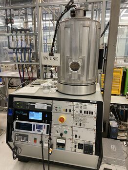
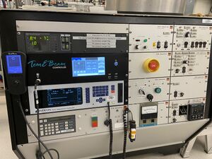
This electron-beam evaporation system is a bell-jar type system and has the capability to do up to 9-4” wafers in a lift-off configuration and up to 18-4” wafers in a sidewall coverage configuration. Rotational motion in combination with baffling is used for lift-off and provides roughly 5% uniformity across a 4” wafer. The sidewall coverage fixturing uses full planetary motion to provide coverage over all sidewalls. The system also an 8-pocket e-beam source and an Inficon IC/5 deposition controller that allows for programming of fully automated multiple layer depositions. The metals available for deposition are Al, Ti, Au, Pt, Ni, Pd, Ag, Ge, Fe, NiCr, NiFe and Cr. This system is used for n-type ohmic contact metalization to compound semiconductors, Schottky contacts to semiconductors, bond pads, and other general metalizations. The maximum deposition thickness during a run is limited to 1.0 microns.
Detailed Specifications
- Temescal 10kV power supply
- 1-Temescal 8-pocket series 260 e-beam sources
- Cryo-pumped system with ~ 5e-7 ultimate base pressure
- Rotation with baffle for 5% uniformity over 4” wafer
- Automatic vacuum sequencing
- Temescal e-beam sweep control
- Inficon IC/5 programmable crystal thickness monitoring system
- Automatic deposition of multiple layer stacks
- Sample size: Pieces or up to 10-4” wafers for lift-off and 24-4” wafers for sidewall coverage
- Metals: Al, Ti, Au, Pt, Ni, Pd, Ag, Ge, Fe, NiCr, NiFe, Cr
Documentation
Materials Table
For the materials tables, please visit the E-Beam Recipe Page.

