Difference between revisions of "Template:News"
(fix feed tags) |
m |
||
| (76 intermediate revisions by 2 users not shown) | |||
| Line 1: | Line 1: | ||
<startfeed /> |
<startfeed /> |
||
| ⚫ | |||
<!-- Description of the RSS feed --> |
<!-- Description of the RSS feed --> |
||
''News from the U.C. Santa Barbara Nanofabrication Facility.'' |
''News from the U.C. Santa Barbara Nanofabrication Facility.'' |
||
| Line 15: | Line 16: | ||
<!----------------------------------------------> |
<!----------------------------------------------> |
||
<!-------- NEWS ITEMS: newest on top --------> |
<!-------- NEWS ITEMS: newest on top --------> |
||
| + | === NanoFab staff awarded Goleta's Innovator of the Year 2023 === |
||
| − | === Metal Processes on the Atomic Layer Deposition === |
||
| + | NanoFab staff member [[Demis D. John]] has been awarded the ''City of Goleta's "Innovator of the Year"'' for 2023! The award stems from the UCSB Nanofab's impact on the communities of Santa Barbara County and surrounding regions, in enabling cutting edge technology companies to thrive, which also enables many local careers in advanced high-tech. See the [https://sbscchamber.com/goletas-finest-2023-award-recipients-announced/ full announcement by the Santa Barbara South Coast Chamber of Commerce]. //[[User:John d|John d]] 13:58, 7 November 2023 (PST) |
||
| − | We now have Ruthenium (Ru) and Platinum (Pt) metal depositions developed on the [[Atomic_Layer_Deposition_(Oxford_FlexAL)|Oxford FlexAL ALD]] tool. See the [[Atomic_Layer_Deposition_Recipes|Atomic Layer Deposition: Recipes]] page or contact [[Bill_Mitchell|Bill Mitchell]] for more information. |
||
| + | === NanoFab Featured in Regional Tech Videos === |
||
| + | The UCSB NanoFab is showcased as a driver of innovation and enabler of the regional high-tech industry. |
||
| + | See the videos here: |
||
| − | === New Deep Silicon Etcher Online === |
||
| + | {| class="wikitable" |
||
| − | A new [[DSEIII_(PlasmaTherm/Deep_Silicon_Etcher)|Plasma-Therm Versaline DSE III DRIE etcher]] has been qualified for bosch etch and single-step etches, and is available for use. The new tool features much higher silicon etch rates, improved uniformity, and allows for photoresist up to the edges of the wafer. |
||
| + | |[https://fast.wistia.net/embed/iframe/l46hsnwg4b?controlsVisibleOnLoad=true&muted=0&playerColor©LinkAndThumbnailEnabled=false '''''Santa Barbara County: This is TechTopia'''''] [[File:Techtopia_Vid_-_Thumbnail_PlayButton.jpg|none|300x300px|link=https://fast.wistia.net/embed/iframe/l46hsnwg4b?controlsVisibleOnLoad=true&muted=0&playerColor©LinkAndThumbnailEnabled=false]] |
||
| + | |[https://www.youtube.com/watch?v=op746os6eRI '''''UCSB NanoFab: An Innovation Center'''''] [[File:NanoFab_COE_Engineering_Vid_-_thumbnail_2_crop.jpg|none|300x300px|link=https://www.youtube.com/watch?v=op746os6eRI]] |
||
| ⚫ | |||
| + | |} |
||
| ⚫ | |||
| + | === CHIPS Act Award Announced to USC and UCSB NanoFab === |
||
| − | === 2016 Survey Results === |
||
| + | [https://carbajal.house.gov/news/documentsingle.aspx?DocumentID=1672 U.S. Congressman Salud Carbajal congratulates UCSB and the NanoFab] on receiving a [https://www.nist.gov/chips CHIPS & Science Act] award, as part of the [https://microelectronicscommons.org/ California DREAMS Hub (Microelectronics Commons) led by USC]. |
||
| − | See the May 2016 {{file|Survey052016.pdf| User Survey Results}}. |
||
| + | // [[User:John d|Demis]] 12:06, 4 October 2023 (PDT) |
||
| + | === JEOL SEM's Installed === |
||
| ⚫ | |||
| + | Both SEM's have been replaced with new JEOL [[SEM_1_(JEOL_IT800SHL)|SEM's #1]] and [[Field_Emission_SEM_2_(JEOL_IT800SHL)|SEM #2]]. SEM#1 has the NABITY lithography system installed, and SEM #2 has always-on EDAX elemental analysis. Contact the [[Aidan_Hopkins|supervisor, Aidan Hopkins]], for more information. |
||
| + | // [[User:John d|John d]] 18:31, 20 September 2023 (PDT) |
||
| + | === Wide FOV Microscope Installed === |
||
| + | We have installed an AmScope stereo microscope in Bay 4 for wide field-of-view digital imaging/capture, with >2cm of FOV currently available. Wiki page here: [[Microscopes#Microscope_.238:_AmScope_Wide_Field_of_View_Stereoscope_.28Bay_4.29|AmScope Wide Field of View Stereoscope]] |
||
| + | // [[User:John d|John d]] 14:52, 19 April 2023 (PDT) |
||
| − | === |
+ | === Loomis Scribe & Break installed === |
| + | We have installed a new [https://loomisinc.com/lsd-155lt/ Loomis LSD-155LT] Automated Scribe & Break Cleaving tool in the Back-End Processing lab. Qualifications are underway. Contact [[Aidan_Hopkins|supervisor, Aidan Hopkins]], for more information. |
||
| − | The [[CAIBE (Oxford Ion Mill)]] is up and running! Contact [[Brian Lingg]] for more information. |
||
| + | // [[User:John d|John d]] 09:41, 16 April 2023 (PDT) |
||
| + | === Dektak XT installed === |
||
| ⚫ | |||
| + | We have replaced the old Dektak 6M with a new Dektak XT profilometer. This tool will provide robust, fast metrology for rapid in-process topography inspection. |
||
| ⚫ | |||
| + | === New Process Control data tables === |
||
| − | |||
| + | We have added [[Process_Group_-_Process_Control_Data|"Process Control Data"]] - data on deposition/etch repeatability - to a number of our highest used etchers and deposition tools. The datasheets are linked in multiple places, mainly on the Recipes pages for each tool, or on the general Recipes pages for [[Vacuum_Deposition_Recipes|'''Deposition Recipes''']] or [[Dry_Etching_Recipes|'''Etch Recipes''']]. |
||
| − | === NanoFiles SFTP Online === |
||
| ⚫ | |||
| − | Files generated with Nanofab tools (SEM images, AFM profiles, etc.) are now available on the nanofab SFTP server. Please check [http://signupmonkey.ece.ucsb.edu SignupMonkey] for details. |
||
| − | |||
| − | [[User:Thibeault|-- ]] 12:00, 07 July 2013 (PST) |
||
<!---------- end of announcements ------------> |
<!---------- end of announcements ------------> |
||
<!----------------------------------------------> |
<!----------------------------------------------> |
||
<!--DO NOT EDIT BELOW THIS LINE--> |
<!--DO NOT EDIT BELOW THIS LINE--> |
||
| + | ===''[[Template:News_-_Older_Articles|See older articles at this link]]''=== |
||
<endfeed /> |
<endfeed /> |
||
<noinclude>[[Category:Templates]]</noinclude> |
<noinclude>[[Category:Templates]]</noinclude> |
||
| ⚫ | |||
Latest revision as of 22:06, 16 November 2023
News from the U.C. Santa Barbara Nanofabrication Facility.
NanoFab staff awarded Goleta's Innovator of the Year 2023
NanoFab staff member Demis D. John has been awarded the City of Goleta's "Innovator of the Year" for 2023! The award stems from the UCSB Nanofab's impact on the communities of Santa Barbara County and surrounding regions, in enabling cutting edge technology companies to thrive, which also enables many local careers in advanced high-tech. See the full announcement by the Santa Barbara South Coast Chamber of Commerce. //John d 13:58, 7 November 2023 (PST)
NanoFab Featured in Regional Tech Videos
The UCSB NanoFab is showcased as a driver of innovation and enabler of the regional high-tech industry.
See the videos here:
Santa Barbara County: This is TechTopia 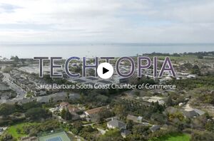 |
UCSB NanoFab: An Innovation Center 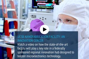 |
// John d 09:26, 1 November 2023 (PST)
CHIPS Act Award Announced to USC and UCSB NanoFab
U.S. Congressman Salud Carbajal congratulates UCSB and the NanoFab on receiving a CHIPS & Science Act award, as part of the California DREAMS Hub (Microelectronics Commons) led by USC. // Demis 12:06, 4 October 2023 (PDT)
JEOL SEM's Installed
Both SEM's have been replaced with new JEOL SEM's #1 and SEM #2. SEM#1 has the NABITY lithography system installed, and SEM #2 has always-on EDAX elemental analysis. Contact the supervisor, Aidan Hopkins, for more information. // John d 18:31, 20 September 2023 (PDT)
Wide FOV Microscope Installed
We have installed an AmScope stereo microscope in Bay 4 for wide field-of-view digital imaging/capture, with >2cm of FOV currently available. Wiki page here: AmScope Wide Field of View Stereoscope // John d 14:52, 19 April 2023 (PDT)
Loomis Scribe & Break installed
We have installed a new Loomis LSD-155LT Automated Scribe & Break Cleaving tool in the Back-End Processing lab. Qualifications are underway. Contact supervisor, Aidan Hopkins, for more information. // John d 09:41, 16 April 2023 (PDT)
Dektak XT installed
We have replaced the old Dektak 6M with a new Dektak XT profilometer. This tool will provide robust, fast metrology for rapid in-process topography inspection. // John d 10:41, 25 January 2023 (PST)
New Process Control data tables
We have added "Process Control Data" - data on deposition/etch repeatability - to a number of our highest used etchers and deposition tools. The datasheets are linked in multiple places, mainly on the Recipes pages for each tool, or on the general Recipes pages for Deposition Recipes or Etch Recipes. // John d 16:07, 5 January 2023 (PST)
See older articles at this link