Difference between revisions of "Suss Aligners (SUSS MJB-3)"
(mentioned that systems are manual, not motorizd.) |
(Added IR Camera SOP) |
||
| Line 53: | Line 53: | ||
==Documentation== |
==Documentation== |
||
| − | *[https://wiki.nanotech.ucsb.edu/wiki/images/d/de/MJB_3_SOP.pdf MJB |
+ | *[https://wiki.nanotech.ucsb.edu/wiki/images/d/de/MJB_3_SOP.pdf MJB-3 Standard Operating Procedure] |
| + | *[https://wiki.nanotech.ucsb.edu/w/images/7/70/MJB_3_IR_Camera_SOP_Rev_B.pdf MJB-3 IR Camera Operation] |
||
===CAD Files=== |
===CAD Files=== |
||
Revision as of 09:38, 26 May 2023
| ||||||||||||||||||||||||||
About
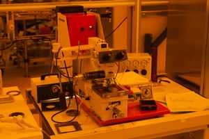
We have two high-performance mask aligners for contact exposure processes. They are manual mechanical systems alignment, contact/proximity, with exposure shuttered by a timer. The resolution (depending on contact mode, optics and exposure wavelength and "operator technique") is into the submicron region. (See descriptions for our "Std." and "IR" units).
Our units are configured for the near-UV window (365 and 405 nm). All units have the "vacuum contact" option extending resolution to ~0.7 microns. Higher resolution optic systems that can be supplied by Suss are given below. The standard soft and hard contact modes of mechanical and pneumatic pressure respectively, give resolution to ~1 micron.
Exposures can be done on substrates from small "piece parts" of less than 1 cm square to substrates of 3 inch diameter or square. Masks up to 4 inches in size can be used although only 3” x 3” of this area is usable. A 4” wafer can be exposed with the system. However, only 3” x 3” will be exposed on the wafer and vacuum mode is unavailable.
Backside Alignment
On the Standard MJB-3, special black chucks may be used for optically transparent materials, allowing you to view through the wafer.
For backside alignment through opaque materials such as Si or GaAs, our IR aligner has backside infrared illumination (halogen bulb) through these black chucks. A Hammamatsu IR camera is installed to view the infrared image.
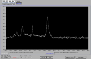
Using a filter, the IR system can be configured for I-line (350 nm) only, assisting in resolution.
Detailed Specifications
- Wafer size: 3" max. for vacuum mode; 4” for soft contact (3” x 3” exposure area)
- Substrate size: 3" x 3" max.
- Wafer / substrate thickness: 0-4.5 mm
- Exposure optics:
- Standard unit (Aligner #1): 350-450 nm/200 W mercury lamp
- IR unit: 280-450 nm/200 W mercury lamp (can filter to 350 nm)
- Additional manufacturer options (none installed on our systems):
- DUV (polychromatic): 240-260 nm/350 W Cd-Xe lamp; 0.2 micron resolution (PMMA)
- DUV (monochromatic): 248 nm/KrF excimer laser; 0.3 micron resolution (PMMA)
- 193 nm/ArF excimer laser; 0.2 micron resolution (PMMA)
- Uniformity:
- ±3% over 2" diameter
- ±5% over 3" diameter
IR Aligner
- Backside illumination with halogen bulb & transparent chuck
- Hammamatsu infrared camera and monitor
- Through-wafer alignment and/or inspection.
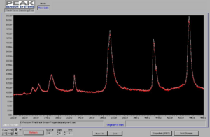
Exposure Optical Spectrum with No Filter
Exposure Optical Spectrum with Filter for i-line Exposure
Documentation
CAD Files
- Male/female alignment marks (GDS): MA6-FrontBack_AlignMarks_only.gds
Recipes
- Recipes > Lithography > Photolithography Recipes > SUSS MJB-3
- Starting recipes for various I-Line photoresists, positive and negative.


