Difference between revisions of "Surface Analysis (KLA/Tencor Surfscan)"
Jump to navigation
Jump to search
(→About) |
(→Documentation: link to SOP (blank)) |
||
| Line 14: | Line 14: | ||
=Documentation= |
=Documentation= |
||
| + | *[[KLA-Tencor Surfscan - Standard Operating Procedure|Standard Operating Procedure]] |
||
*[[media:Surfscan-Operation-Manual.pdf|Operations Manual]] |
*[[media:Surfscan-Operation-Manual.pdf|Operations Manual]] |
||
| + | **''For detailed measurement info, it is highly recommended that you read the manual.'' |
||
*[[media:Surfscan-Surfscan 6200 info.pdf|Surfscan Info]] |
*[[media:Surfscan-Surfscan 6200 info.pdf|Surfscan Info]] |
||
*[[Surfscan6200 photos]] |
*[[Surfscan6200 photos]] |
||
Revision as of 15:09, 25 March 2019
|
About
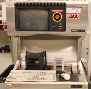
This system uses a laser-based scattering method to count size and distribution of particles (or other scattering defects) on a flat wafer surface. It can scan wafers in size from 4 to 6 inches.
Documentation
- Standard Operating Procedure
- Operations Manual
- For detailed measurement info, it is highly recommended that you read the manual.
- Surfscan Info
- Surfscan6200 photos
