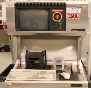
Difference between revisions of "Surface Analysis (KLA/Tencor Surfscan)"
Jump to navigation
Jump to search
| (73 intermediate revisions by 4 users not shown) | |||
| Line 1: | Line 1: | ||
| − | {{ |
+ | {{tool2|{{PAGENAME}} |
|picture=KLA.jpg |
|picture=KLA.jpg |
||
|type = Inspection, Test and Characterization |
|type = Inspection, Test and Characterization |
||
|super= Biljana Stamenic |
|super= Biljana Stamenic |
||
| + | |super2= Don Freeborn |
||
|location=Bay 5 |
|location=Bay 5 |
||
|description = Surface Analysis |
|description = Surface Analysis |
||
| − | + | KLA/Tencor Surfscan |
|
|manufacturer = Tencor |
|manufacturer = Tencor |
||
|materials = |
|materials = |
||
|toolid= |
|toolid= |
||
}} |
}} |
||
| − | =About= |
+ | ==About== |
| − | This system uses a laser-based scattering method to count size and distribution of particles (or other scattering defects) on a flat wafer surface. |
+ | This system uses a laser-based scattering method to count size and distribution of particles (or other scattering defects) on a flat wafer surface. |
| + | It can scan wafers in size from 4 to 8 inches. Piece-parts are more difficult but can be scanned with a custom recipe. |
||
| ⚫ | |||
| + | |||
| ⚫ | |||
| + | 4-inch wafers are the most standard size to measure. |
||
| − | *[[media:Surfscan-Surfscan 6200 info.pdf|Surfscan Info]] |
||
| + | |||
| − | *[[Surfscan6200 photos]] |
||
| + | For measuring very low particle counts accurately, purchase "low particle count" (LPC) wafers from a Silicon wafer vendor, and keep the wafers in the case and clean at all times until use. |
||
| + | |||
| ⚫ | |||
| + | |||
| + | ===Operating Procedures=== |
||
| + | |||
| + | |||
| + | *[https://wiki.nanofab.ucsb.edu/w/images/a/a2/SURFSCAN_6200_122123_for_8inch_wafers.pdf Surfscan 6200 8inch wafers] * |
||
| + | *[https://wiki.nanofab.ucsb.edu/w/images/1/1a/SURFSCAN_6200_122023_for_6inch_wafers.pdf Surfscan 6200 6inch wafers] * |
||
| + | *[https://wiki.nanofab.ucsb.edu/w/images/9/9f/SURFSCAN_6200_122123_for_4inch_wafers.pdf Surfscan 6200 4inch wafers] * |
||
| + | *[https://wiki.nanofab.ucsb.edu/w/images/a/a7/SURFSCAN_6200_122123_small_substrates.pdf Surfscan 6200 [Small samples, and 2inch and 3inch wafers]] * |
||
| + | |||
| + | **''You must water-mount your small sample or wafer(2inch or 3 inch) to a 4-inch wafer.'' |
||
| + | *[[Wafer scanning process traveler|Wafer Particle Count - Process Traveler]] |
||
| + | |||
| + | *[https://wiki.nanofab.ucsb.edu/w/images/2/29/Wafer_Particle_Count-Process_Traveler.pdf Wafer Scanning Instructions] |
||
| + | **''This is the procedure Staff uses to calibrate particle counts on our deposition tools.'' |
||
| + | |||
| + | ===Other Documentation=== |
||
| + | |||
| ⚫ | |||
| + | **''For detailed measurement info, it is highly recommended that you read the manual.'' |
||
| + | |||
| + | *[[Glossary]] |
||
| + | *[[Surfscan Errors and Workarounds|Common Errors & Workarounds]] |
||
| + | |||
| + | ==Examples== |
||
| + | {| class="wikitable" |
||
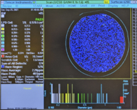
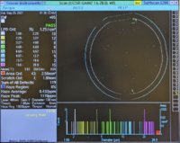
| + | |+A low-particle 4-inch wafer example: |
||
| + | !Gain 4: Small Particles |
||
| + | (0.160µm – 1.60µm) |
||
| + | !Gain 2: Large Particles |
||
| + | (1.60µm – 28.0µm) |
||
| + | |- |
||
| + | |[[File:Surfscan Low-Particle Example - G4.png|frameless|200x200px]] |
||
| + | |[[File:Surfscan Low-Particle Example - G2.png|frameless|200x200px]] |
||
| + | |} |
||
| + | {| class="wikitable" |
||
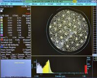
| + | |+A high-particle 4-inch wafer example: |
||
| + | !Gain 4: Small Particles |
||
| + | (0.160µm – 1.60µm) |
||
| + | !Gain 2: Large Particles |
||
| + | (1.60µm – 28.0µm) |
||
| + | |- |
||
| + | |[[File:Surfscan - 230113A7 Gain4 high particles.jpg|frameless|199x199px]] |
||
| + | |[[File:Surfscan 230113A7G2 after low particles.jpg|frameless|195x195px]] |
||
| + | |} |
||
Latest revision as of 18:02, 2 February 2024
| ||||||||||||||||||||||||||
About
This system uses a laser-based scattering method to count size and distribution of particles (or other scattering defects) on a flat wafer surface.
It can scan wafers in size from 4 to 8 inches. Piece-parts are more difficult but can be scanned with a custom recipe.
4-inch wafers are the most standard size to measure.
For measuring very low particle counts accurately, purchase "low particle count" (LPC) wafers from a Silicon wafer vendor, and keep the wafers in the case and clean at all times until use.
Documentation
Operating Procedures
- Surfscan 6200 8inch wafers *
- Surfscan 6200 6inch wafers *
- Surfscan 6200 4inch wafers *
- Surfscan 6200 [Small samples, and 2inch and 3inch wafers] *
- You must water-mount your small sample or wafer(2inch or 3 inch) to a 4-inch wafer.
- Wafer Particle Count - Process Traveler
- Wafer Scanning Instructions
- This is the procedure Staff uses to calibrate particle counts on our deposition tools.
Other Documentation
- Operations Manual
- For detailed measurement info, it is highly recommended that you read the manual.
Examples
| Gain 4: Small Particles
(0.160µm – 1.60µm) |
Gain 2: Large Particles
(1.60µm – 28.0µm) |
|---|---|
|
|
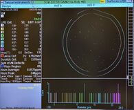
| Gain 4: Small Particles
(0.160µm – 1.60µm) |
Gain 2: Large Particles
(1.60µm – 28.0µm) |
|---|---|
|
|
