Difference between revisions of "Stepper 3 (ASML DUV)"
| (26 intermediate revisions by the same user not shown) | |||
| Line 15: | Line 15: | ||
==About== |
==About== |
||
| + | ===General Capabilities/Overview=== |
||
| − | The ASML 5500 stepper is a 248nm DUV stepper for imaging dense features down to below 200nm and isolated line structures down to below 150nm. |
+ | The ASML 5500 stepper is a 248nm (KrF) DUV stepper for imaging dense features down to below 200nm and isolated line structures down to below 150nm (with effort). 300nm+ features are relatively "easy" to resolve. Layer-to-layer overlay accuracy is better than 30nm. |
| − | The system is configured for 4” wafers |
+ | The system is configured for 4” wafers. The system is designed for high throughput, so shooting multiple 4" wafers is extremely fast, typically minutes per wafer, but any size other than 4-inch is difficult to work with (see below for more info). Additionally, exposure jobs are highly programmable, allowing for very flexible exposures of multiple aligned patterns from multiple masks/reticles in a single session, allowing for process optimization of large vs. small features in a single lithography. |
The full field useable exposure area is limited to the intersection of a 31mm diameter circle and a rectangle of dimensions 22mm x 27mm. Users have stitched multiple photomasks together with success. See the [[ASML 5500 Mask Making Guidelines|Mask Making Guidelines page]] for more info on exposure field sizes and how to order your mask plates. |
The full field useable exposure area is limited to the intersection of a 31mm diameter circle and a rectangle of dimensions 22mm x 27mm. Users have stitched multiple photomasks together with success. See the [[ASML 5500 Mask Making Guidelines|Mask Making Guidelines page]] for more info on exposure field sizes and how to order your mask plates. |
||
| + | '''Tutorial:''' If you are not familiar with the differences between Contact Litho and Stepper Litho, please review this short tutorial: [https://wiki.nanofab.ucsb.edu/w/images/c/cb/Demis_D_John_-_Stepper_Reticle_Layout_vs_Wafer_Layout.pdf Demis D. John - Stepper_Reticle_Layout_vs_Wafer_Layout.pdf] |
||
| ⚫ | |||
| + | |||
| + | ===Photoresists Available=== |
||
| ⚫ | |||
*UV210-0.3 - Positive: 300nm nominal thickness |
*UV210-0.3 - Positive: 300nm nominal thickness |
||
| Line 32: | Line 36: | ||
AZ300MIF Developer for all processes |
AZ300MIF Developer for all processes |
||
| + | |||
| + | Many of these DUV PR's are also able to be exposed with [[E-Beam Lithography System (JEOL JBX-6300FS)|EBL]]. |
||
| + | |||
| + | ===Part Size Limits=== |
||
| + | With staff support, mounted pieces down to 14mm in size can be exposed using a 4” wafer as a carrier. Flatness will typically be worse in this situation, so small <<500nm features will usually have bad uniformity across the mounted part due to focus variations. Edge bead on irregular pieces (eg. quarter-wafers/squares) will significantly reduce yield/uniformity. |
||
| + | |||
| + | Multi-layer Alignment on mounted parts is particularly difficult, requiring either semi-permanent mounting to the carrier (eg. BCB, SU8 etc.) or significant difficulty/effort to re-align the part to the carrier wafer on each lithography (≤100µm re-mounting accuracy needed). |
||
| + | |||
| + | At this time the maximum wafer size is 4” (100mm) wafers with SEMI standard wafer flat (not Notch). |
||
| + | |||
| + | ===Service Provider=== |
||
| + | |||
| ⚫ | |||
==Process Information== |
==Process Information== |
||
| Line 37: | Line 54: | ||
*[https://wiki.nanotech.ucsb.edu/w/index.php?title=Lithography_Recipes#Photolithography_Recipes '''Process Recipes Page'''] '''> "Stepper 3"''' - ''Established recipes and corresponding linewidths, photoresists etc.'' |
*[https://wiki.nanotech.ucsb.edu/w/index.php?title=Lithography_Recipes#Photolithography_Recipes '''Process Recipes Page'''] '''> "Stepper 3"''' - ''Established recipes and corresponding linewidths, photoresists etc.'' |
||
*Sample size: 100 mm wafers with SEMI std. major flat |
*Sample size: 100 mm wafers with SEMI std. major flat |
||
| − | **''Piece-parts process is possible but difficult - contact |
+ | **''Piece-parts process is possible but difficult - contact supervisor for info'' |
*Alignment Accuracy: < 50 nm |
*Alignment Accuracy: < 50 nm |
||
*Minimum Feature Size: ≤150 nm isolated lines, ≤200 nm dense patterns |
*Minimum Feature Size: ≤150 nm isolated lines, ≤200 nm dense patterns |
||
**''To achieve ≤200nm features with high uniformity, we recommend wafers with total thickness variation (TTV) ≤5µm, and designing your CAD with a smaller Image Size for the high-res. feature''. |
**''To achieve ≤200nm features with high uniformity, we recommend wafers with total thickness variation (TTV) ≤5µm, and designing your CAD with a smaller Image Size for the high-res. feature''. |
||
| − | * |
+ | *Wafer Thickness: Minimum ≈ 200µm, Maximum ≈ 1.1 mm |
| − | *Maximum |
+ | *Maximum Dose: ~100mJ |
| + | **''Non-chemically amplified EBL resists are not permissible due to this limit.'' |
||
| ⚫ | |||
| − | == |
+ | ===Maximum Wafer Bow=== |
| + | Measured over 90mm on the [[Film Stress (Tencor Flexus)|Tencor Flexus]] |
||
| + | *'''Do not run wafers with bow values higher than the following values''', contact supervisor for advice if needed. |
||
| − | *[[ASML Stepper 3 Standard Operating Procedure|Standard Operating Procedures]] - ''Exposing wafers, loading reticles, focus/exposure matrix'' |
||
| + | *Silicon wafers (~550µm thick): 100 µm will likely fail. |
||
| − | **[[ASML Stepper 3 Standard Operating Procedure#Running a focus and.2For exposure matrix|Focus-Exposure Matrix]] - ''used for'' ''calibrating sensitive exposure parameters'' |
||
| + | *Sapphire (less pliable), ≥60µm bow will intermittently fail - DO NOT RUN |
||
| − | *[[ASML Stepper 3 Error Recovery, Troubleshooting and Calibration|Error Recovery, Troubleshooting & Calibration Check]] |
||
| + | **This applies especially for GaN-on-Sapphire, which often have high wafer bow. |
||
| − | **''Common errors/solutions, System Calibration Verification (aka. IQC)'' |
||
| ⚫ | |||
| + | *''Substrate material and substrate thickness affect this limit - please contact [[Demis D. John|supervisor]] for advice.'' |
||
| + | *You can stress-compensate wafers to reduce the wafer bow, eg. via underside dep. of [[Sputtering Recipes#Si3N4 deposition .28IBD.29|IBD SiN]], or other compressive/tensile films for concave-down/up bow, respectively. |
||
| + | ==Operating Procedures== |
||
| − | *[[ASML 5500: Recovering from an Error|ASML 5500: Recovering from an Error+Wafer Retrieval]] |
||
| + | <code>'''All operating procedures and reticle guides have been access-restricted only to trained users, by vendor request. Please contact [[Demis D. John|supervisor]] for more info.'''</code> |
||
| − | **''How to abort the job and recover your wafer.'' |
||
| − | *[//wiki.nanotech.ucsb.edu/wiki/images/c/cd/ASML_Job_Set-Up_Guide_simple_v1.pdf Job Programming- Simplified - Full Wafers] |
||
| − | *[//wiki.nanotech.ucsb.edu/wiki/images/f/f7/ASML_Job_Set-Up_Guide_v2.pdf Job Programming - Full] |
||
| + | *[https://drive.google.com/drive/folders/1U9-03qU2htQp_5x39LNq-mn5Q3vXXLDf?usp=drive_link '''<u>ASML Operating Procedures</u>'''] - shared google drive folder of PAS 5500/300 operating procedures. |
||
| − | *[[ASML Stepper 3 - Substrates smaller than 100mm/4-inch|Working with Substrates Smaller than 100mm/4-inch]] |
||
| + | **''You must log into google-drive with your UCSB NetID to access this folder.'' |
||
| + | **''Please contact the [[Demis D. John|tool supervisor]] if you need access.'' |
||
| + | ===Training Procedure=== |
||
| ⚫ | |||
| + | To get access to this tool, please do the following: |
||
| − | **''All the info you need to design and order a reticle for this system.'' |
||
| + | |||
| + | #Email the [[Demis D. John|supervisor]] for access to the training video. Please provide your UCSB NetID. |
||
| + | #Study the training videos below. |
||
| + | ##If you are a technician and will never program jobs, only Part 1 is necessary. |
||
| + | #"Shadow" someone in your group who uses the machine, <u>until you are completely comfortable</u> with wafer cleaning (critical), reticle load/unload and running a pre-made job. When you are ready do step 3: |
||
| + | #Contact [[Demis D. John|the supervisor]] for an short hands-on check-off, after which you'll get signupmonkey access. |
||
===Online Video Trainings=== |
===Online Video Trainings=== |
||
| + | The video trainings are only accessible to authorized users per vendor request. Email the [[Demis D. John|supervisor]] for access. |
||
| + | |||
''These video trainings have bookmarks to skip to specific sections - use them as reference.'' |
''These video trainings have bookmarks to skip to specific sections - use them as reference.'' |
||
''Remember, you are NOT authorized to use the system until a [[Demis D. John|supervisor]] grants you access.'' |
''Remember, you are NOT authorized to use the system until a [[Demis D. John|supervisor]] grants you access.'' |
||
| + | {| class="wikitable" |
||
| + | | colspan="2" |To view the vids: after clicking the below link, |
||
| + | choose "'''Canvas'''" from the dropdown and then |
||
| + | |||
| + | click "'''UCSB Users'''" and login with your '''UCSB NetID'''. |
||
| + | |- |
||
| + | |[[File:2024-01 PanOpto - Canvas dropdown.png|alt=screenshot of dropdown list showing "canvas" option|frameless]] |
||
| + | |[[File:2024-01 PanOpto - UCSB Login.png|alt=screenshot of "UCSB users" login button|frameless|135x135px]] |
||
| + | |} |
||
| + | '''Training Vids:''' |
||
*[https://gauchocast.hosted.panopto.com/Panopto/Pages/Viewer.aspx?id=798e5110-0823-4abd-9458-ac5c01855a99 Part 1: System Info & Running a Job] |
*[https://gauchocast.hosted.panopto.com/Panopto/Pages/Viewer.aspx?id=798e5110-0823-4abd-9458-ac5c01855a99 Part 1: System Info & Running a Job] |
||
| Line 72: | Line 111: | ||
==Design Tools== |
==Design Tools== |
||
| + | ===Mask Design and CAD files=== |
||
| − | *[[ASML 5500 Mask Making Guidelines|Mask Making Guidelines]] - All the info you need to design and order a reticle for this system. |
||
| ⚫ | |||
| − | *[https://github.com/demisjohn/ASML_JobCreator ASML Job Creator] - Python scripts for generating ASML Job Files. |
||
| ⚫ | |||
| ⚫ | |||
| ⚫ | |||
| − | ===Software Options=== |
||
| ⚫ | |||
| − | ''The Following software options have been installed on the machine.'' |
||
| ⚫ | |||
| + | *See the [[Calculators + Utilities#CAD%20Files%20.26%20Templates|Calculators + Utilities > CAD Files & Templates]] page for other useful CAD files, such as overlay verniers, vented fonts etc. |
||
| + | ===UCSB Photomasks Available=== |
||
| − | *[[ASML Stepper 3 - Shifted Measurement Scans (SMS)|Shifted Measurement Scans]] - better tilt/level measurement locations for edge-die. Simply enable the Checkbox in your job file. |
||
| + | |||
| − | *[[ASML Stepper 3 - Compound Image Design (CIDS)|Compound Image Design]] - flexible Image Distribution: grouping of Images with shifts, duplicate instances of Images in each Cell. |
||
| ⚫ | |||
| − | *[[ASML Stepper 3 - Job Creator|Job Creator]] - create binary ASML job files from ASCII text files. Python scripting capabilities using this option are currently implemented, contact [[Demis D. John|the supervisor]] for more info. |
||
==Recipes== |
==Recipes== |
||
| Line 90: | Line 127: | ||
Litho. recipes for all our photolith. tools can be found on the [[Lithography Recipes#Photolithography Recipes|Photolithography Recipes]] page. |
Litho. recipes for all our photolith. tools can be found on the [[Lithography Recipes#Photolithography Recipes|Photolithography Recipes]] page. |
||
| − | == |
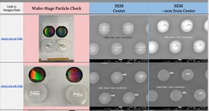
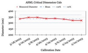
+ | ==Process Control Data== |
| + | *''The Process Group regularly measures data on lithography Critical Dimension ("CD") and Wafer-stage Particulate Contamination for this tool, using a sensitive lithography process that will reveal small changes in Dose repeatability and wafer flatness.'' |
||
| ⚫ | |||
| + | *[https://docs.google.com/spreadsheets/d/1xW1TFH_QjPMWl9T1jiKzwmYe4B2wg7KY-nqOKUoXttI/edit#gid=0 '''Data Table for CD Uniformity and Particulate Contamination'''] |
||
| + | *[https://docs.google.com/spreadsheets/d/1xW1TFH_QjPMWl9T1jiKzwmYe4B2wg7KY-nqOKUoXttI/edit#gid=1804752281 '''Plots of CD Repeatability'''] |
||
| + | |||
| + | {| |
||
| + | |[[File:ASML CD Cals - Example Table.jpg|alt=ASML CD Calibration data - Screenshot of Table|none|thumb|300x300px|''Example of Data Table with SEM's of 320nm features. [https://docs.google.com/spreadsheets/d/1xW1TFH_QjPMWl9T1jiKzwmYe4B2wg7KY-nqOKUoXttI/edit#gid=0 Click for full data table.]''|link=https://docs.google.com/spreadsheets/d/1xW1TFH_QjPMWl9T1jiKzwmYe4B2wg7KY-nqOKUoXttI/edit#gid=0]] |
||
| + | |[[File:ASML CD Cals - Example Plot.jpg|alt=ASML CD Calibration Data - Screenshot of SPC Plot|none|thumb|''Example SPC Chart - Measured Critical Dimension "CD" versus Date. [https://docs.google.com/spreadsheets/d/1xW1TFH_QjPMWl9T1jiKzwmYe4B2wg7KY-nqOKUoXttI/edit#gid=1804752281 Click for charts.]''|link=https://docs.google.com/spreadsheets/d/1xW1TFH_QjPMWl9T1jiKzwmYe4B2wg7KY-nqOKUoXttI/edit#gid=1804752281]] |
||
| + | |} |
||
| + | <br /> |
||
Latest revision as of 17:00, 9 April 2024
| |||||||||||||||||||||||

About
General Capabilities/Overview
The ASML 5500 stepper is a 248nm (KrF) DUV stepper for imaging dense features down to below 200nm and isolated line structures down to below 150nm (with effort). 300nm+ features are relatively "easy" to resolve. Layer-to-layer overlay accuracy is better than 30nm.
The system is configured for 4” wafers. The system is designed for high throughput, so shooting multiple 4" wafers is extremely fast, typically minutes per wafer, but any size other than 4-inch is difficult to work with (see below for more info). Additionally, exposure jobs are highly programmable, allowing for very flexible exposures of multiple aligned patterns from multiple masks/reticles in a single session, allowing for process optimization of large vs. small features in a single lithography.
The full field useable exposure area is limited to the intersection of a 31mm diameter circle and a rectangle of dimensions 22mm x 27mm. Users have stitched multiple photomasks together with success. See the Mask Making Guidelines page for more info on exposure field sizes and how to order your mask plates.
Tutorial: If you are not familiar with the differences between Contact Litho and Stepper Litho, please review this short tutorial: Demis D. John - Stepper_Reticle_Layout_vs_Wafer_Layout.pdf
Photoresists Available
See PhotoLith. Recipes for full process info & links to PR datasheets.
- UV210-0.3 - Positive: 300nm nominal thickness
- UV6-0.8 - Positive: 800nm nominal thickness
- UV26-2.5 - Positive: 2.5um nominal thickness
- UVN2300-0.5 - Negative: 500nm nominal thickness
- DUV42P-6/DS-K101 - Bottom Anti-Reflective Coatings “BARC”
- PMGI/LOL1000/LOL2000 - Underlayers
AZ300MIF Developer for all processes
Many of these DUV PR's are also able to be exposed with EBL.
Part Size Limits
With staff support, mounted pieces down to 14mm in size can be exposed using a 4” wafer as a carrier. Flatness will typically be worse in this situation, so small <<500nm features will usually have bad uniformity across the mounted part due to focus variations. Edge bead on irregular pieces (eg. quarter-wafers/squares) will significantly reduce yield/uniformity.
Multi-layer Alignment on mounted parts is particularly difficult, requiring either semi-permanent mounting to the carrier (eg. BCB, SU8 etc.) or significant difficulty/effort to re-align the part to the carrier wafer on each lithography (≤100µm re-mounting accuracy needed).
At this time the maximum wafer size is 4” (100mm) wafers with SEMI standard wafer flat (not Notch).
Service Provider
- ASML - ASML performs quarterly periodic maintenance and provides on-demand support.
Process Information
- Process Recipes Page > "Stepper 3" - Established recipes and corresponding linewidths, photoresists etc.
- Sample size: 100 mm wafers with SEMI std. major flat
- Piece-parts process is possible but difficult - contact supervisor for info
- Alignment Accuracy: < 50 nm
- Minimum Feature Size: ≤150 nm isolated lines, ≤200 nm dense patterns
- To achieve ≤200nm features with high uniformity, we recommend wafers with total thickness variation (TTV) ≤5µm, and designing your CAD with a smaller Image Size for the high-res. feature.
- Wafer Thickness: Minimum ≈ 200µm, Maximum ≈ 1.1 mm
- Maximum Dose: ~100mJ
- Non-chemically amplified EBL resists are not permissible due to this limit.
Maximum Wafer Bow
Measured over 90mm on the Tencor Flexus
- Do not run wafers with bow values higher than the following values, contact supervisor for advice if needed.
- Silicon wafers (~550µm thick): 100 µm will likely fail.
- Sapphire (less pliable), ≥60µm bow will intermittently fail - DO NOT RUN
- This applies especially for GaN-on-Sapphire, which often have high wafer bow.
- Near these values, and you may lose the wafer inside the machine due to wafer vacuum error - DO NOT RUN if unsure.
- Substrate material and substrate thickness affect this limit - please contact supervisor for advice.
- You can stress-compensate wafers to reduce the wafer bow, eg. via underside dep. of IBD SiN, or other compressive/tensile films for concave-down/up bow, respectively.
Operating Procedures
All operating procedures and reticle guides have been access-restricted only to trained users, by vendor request. Please contact supervisor for more info.
- ASML Operating Procedures - shared google drive folder of PAS 5500/300 operating procedures.
- You must log into google-drive with your UCSB NetID to access this folder.
- Please contact the tool supervisor if you need access.
Training Procedure
To get access to this tool, please do the following:
- Email the supervisor for access to the training video. Please provide your UCSB NetID.
- Study the training videos below.
- If you are a technician and will never program jobs, only Part 1 is necessary.
- "Shadow" someone in your group who uses the machine, until you are completely comfortable with wafer cleaning (critical), reticle load/unload and running a pre-made job. When you are ready do step 3:
- Contact the supervisor for an short hands-on check-off, after which you'll get signupmonkey access.
Online Video Trainings
The video trainings are only accessible to authorized users per vendor request. Email the supervisor for access.
These video trainings have bookmarks to skip to specific sections - use them as reference.
Remember, you are NOT authorized to use the system until a supervisor grants you access.
| To view the vids: after clicking the below link,
choose "Canvas" from the dropdown and then click "UCSB Users" and login with your UCSB NetID. | |

|

|
Training Vids:
Design Tools
Mask Design and CAD files
- Mask Making Guidelines - All the info you need to design and order a reticle for this system.
- Access is restricted to trained users only - please contact tool supervisor for access.
- Templates and CAD help - (on the above page) CAD files and spreadsheets to help you design/program.
- See the Calculators + Utilities > CAD Files & Templates page for other useful CAD files, such as overlay verniers, vented fonts etc.
UCSB Photomasks Available
- UCSB DUV Reticles - Photomasks available with various Alignment Markers (contact, EBL), Resolution Testing etc.
Recipes
See the Recipes > Lithography > Stepper Recipes > Stepper #3 page for starting processes for various photoresists, including Dose/Focus values.
Litho. recipes for all our photolith. tools can be found on the Photolithography Recipes page.
Process Control Data
- The Process Group regularly measures data on lithography Critical Dimension ("CD") and Wafer-stage Particulate Contamination for this tool, using a sensitive lithography process that will reveal small changes in Dose repeatability and wafer flatness.
- Data Table for CD Uniformity and Particulate Contamination
- Plots of CD Repeatability
 Example of Data Table with SEM's of 320nm features. Click for full data table. |
 Example SPC Chart - Measured Critical Dimension "CD" versus Date. Click for charts. |