Difference between revisions of "SEM Sample Coater (Hummer)"
Jump to navigation
Jump to search
(Created page with "{{tool|{{PAGENAME}} |picture=SEMSample.jpg |type = Inspection, Test and Characterization |super= Tony Bosch |location=Bay 1 |description = |manufacturer = Hummer |materials = |…") |
(trying "tool2" template) |
||
| (3 intermediate revisions by 3 users not shown) | |||
| Line 1: | Line 1: | ||
| − | {{ |
+ | {{tool2|{{PAGENAME}} |
|picture=SEMSample.jpg |
|picture=SEMSample.jpg |
||
|type = Inspection, Test and Characterization |
|type = Inspection, Test and Characterization |
||
| − | |super= |
+ | |super= Don Freeborn |
|location=Bay 1 |
|location=Bay 1 |
||
|description = |
|description = |
||
| Line 9: | Line 9: | ||
|toolid= |
|toolid= |
||
}} |
}} |
||
| + | =About= |
||
| + | This system is for coating Pd/Au thin layers onto samples that will charge during FESEM inspection. |
||
| + | |||
| + | === When to use === |
||
| + | If you tried SEM'ing a sample, and the sample appears to drift/move during imaging/capture, or astigmatism is constantly changing, then your sample may be charging up and deflecting the electron beams. This is common for imaging insulators such as substrates made of glass (SiO2), or substrates coated in glass (SiO2, SiN) or thick photoresist (≥1µm). Thin layers (<<1µm) on top of conductive substrates (eg. 200nm SiO2 on Silicon substrate) can often allow electron beams and fields to penetrate to the conductor, possibly not requiring AuPd coating. |
||
| + | |||
| + | == Operating Procedures == |
||
| + | {{Todo|Upload SOP. Printouts available at tool.}} |
||
| + | |||
| + | * [[Hummer SEM Sample Coater - Techniques to reduce charging in SEMs|Techniques to reduce charging in SEMs]] |
||
| + | |||
| + | <br /> |
||
Revision as of 06:48, 22 June 2022
| ||||||||||||||||||||
About
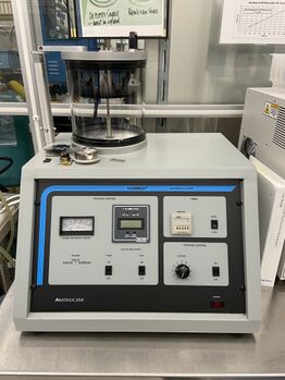
This system is for coating Pd/Au thin layers onto samples that will charge during FESEM inspection.
When to use
If you tried SEM'ing a sample, and the sample appears to drift/move during imaging/capture, or astigmatism is constantly changing, then your sample may be charging up and deflecting the electron beams. This is common for imaging insulators such as substrates made of glass (SiO2), or substrates coated in glass (SiO2, SiN) or thick photoresist (≥1µm). Thin layers (<<1µm) on top of conductive substrates (eg. 200nm SiO2 on Silicon substrate) can often allow electron beams and fields to penetrate to the conductor, possibly not requiring AuPd coating.
Operating Procedures
| To Do: Upload SOP. Printouts available at tool. |
