Difference between revisions of "Resistivity Mapper (CDE RESMAP)"
Jump to navigation
Jump to search
(link to quick-start instructions page) |
|||
| Line 11: | Line 11: | ||
}} |
}} |
||
= About = |
= About = |
||
| − | The CDE Resmap 4 point resistivity mapper is used for measuring resistivity across the wafer for substrates and thin films deposited in the facility. The system can do automated resistivity mapping for pieces to 8 inch wafers. |
+ | The CDE Resmap 4 point resistivity mapper is used for measuring resistivity across the wafer for substrates and thin films deposited in the facility. The system can do automated resistivity mapping for pieces to 8 inch wafers. |
| + | |||
| + | The resistivity range is 2 mOhm/Square to 5 MOhm/square. Contour plots, 3D plots, histograms, data exporting are supported from the Windows XP based control system. |
||
| + | |||
| + | == Instructions == |
||
| + | * [[CDE ResMap Quick-Start instructions]] |
||
Revision as of 12:42, 17 April 2018
|
About
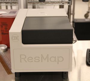
The CDE Resmap 4 point resistivity mapper is used for measuring resistivity across the wafer for substrates and thin films deposited in the facility. The system can do automated resistivity mapping for pieces to 8 inch wafers.
The resistivity range is 2 mOhm/Square to 5 MOhm/square. Contour plots, 3D plots, histograms, data exporting are supported from the Windows XP based control system.
