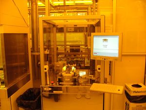
Difference between revisions of "Plasma Activation (EVG 810)"
Jump to navigation
Jump to search
(Created page with "{{tool|{{PAGENAME}} |picture=EVG.jpg |type = Dry Etch |super= Aidan Hopkins |phone= 805-893-3918x208 |location=Bay 7 |email=hopkins@ece.ucsb.edu |description = Plasma Surface Act…") |
(SOP rev) |
||
| (15 intermediate revisions by 6 users not shown) | |||
| Line 1: | Line 1: | ||
| − | {{ |
+ | {{tool2|{{PAGENAME}} |
|picture=EVG.jpg |
|picture=EVG.jpg |
||
|type = Dry Etch |
|type = Dry Etch |
||
| − | |super= |
+ | |super= Lee Sawyer |
| + | |super2= Aidan Hopkins |
||
| − | |phone= 805-893- |
+ | |phone= 805-893-2123 |
|location=Bay 7 |
|location=Bay 7 |
||
| − | |email= |
+ | |email=lee_sawyer@ucsb.edu |
|description = Plasma Surface Activation |
|description = Plasma Surface Activation |
||
|manufacturer = EVG Group |
|manufacturer = EVG Group |
||
|materials = |
|materials = |
||
| + | |toolid=29 |
||
}} |
}} |
||
| − | = |
+ | ==About== |
This a capacitively coupled Oxygen plasma activation system used exclusively for the surface activation of clean surfaces prior to wafer bonding. This technique allows bonding temperatures to be lowered and is used as a companion tool to the Karl-Suss SB6 wafer bond tool. |
This a capacitively coupled Oxygen plasma activation system used exclusively for the surface activation of clean surfaces prior to wafer bonding. This technique allows bonding temperatures to be lowered and is used as a companion tool to the Karl-Suss SB6 wafer bond tool. |
||
| − | = |
+ | ==Detailed Specifications== |
*Gases used: O<sub>2</sub> and N<sub>2</sub> |
*Gases used: O<sub>2</sub> and N<sub>2</sub> |
||
*Sample size: pieces to 6” wafer |
*Sample size: pieces to 6” wafer |
||
| + | *Recipes characterized for substrate thicknesses between 250um and 750um. Thicknesses outside of this range need to have parameters optimized to minimize reflective power. |
||
| + | |||
| + | ==Documentation== |
||
| + | |||
| + | *[https://wiki.nanofab.ucsb.edu/w/images/2/21/EVG_Plasma_Activation_SOP_Rev_E.pdf Plasma Activation Standard Operating Procedure] |
||
| + | *[https://wiki.nanotech.ucsb.edu/wiki/images/9/93/EVG_Plasma_Activation_Recipe_Copying.pdf How to copy recipes] |
||
| + | |||
| + | ==Recipes== |
||
| + | Please see the [[Oxygen Plasma System Recipes#Plasma Activation .28EVG 810.29|Oxygen Plasma Recipe]] page for standard EVG recipes. |
||
Latest revision as of 11:06, 30 October 2023
| ||||||||||||||||||||||||||||||
About
This a capacitively coupled Oxygen plasma activation system used exclusively for the surface activation of clean surfaces prior to wafer bonding. This technique allows bonding temperatures to be lowered and is used as a companion tool to the Karl-Suss SB6 wafer bond tool.
Detailed Specifications
- Gases used: O2 and N2
- Sample size: pieces to 6” wafer
- Recipes characterized for substrate thicknesses between 250um and 750um. Thicknesses outside of this range need to have parameters optimized to minimize reflective power.
Documentation
Recipes
Please see the Oxygen Plasma Recipe page for standard EVG recipes.
