Difference between revisions of "PECVD Recipes"
| (271 intermediate revisions by 3 users not shown) | |||
| Line 1: | Line 1: | ||
{{recipes|Vacuum Deposition}} |
{{recipes|Vacuum Deposition}} |
||
| + | |||
=[[PECVD 1 (PlasmaTherm 790)]]= |
=[[PECVD 1 (PlasmaTherm 790)]]= |
||
| − | Note: Software upgrade performed on 2018-10-10. Note any changes in film. |
||
| + | ===[https://docs.google.com/spreadsheets/d/1fTDNXxpf4tgNYLIEs_jvehG1KvtXqqTRDBI7sHNAVvo/edit#gid=1270764394 PECVD 1 Process Control Plots] - Plots of all process control data=== |
||
| − | ==== Historical Particulate Data ==== |
||
| + | ==SiO<sub>2</sub> deposition (PECVD #1)== |
||
| − | *[https://docs.google.com/spreadsheets/d/1a0XrY6HuJ6L9niThZYI-u4XH69Hnbe3jkm1qKmrR8Rg/edit#gid=sharing Particulates(Gain4) in PECVD#1-OLD DATA 2015] |
||
| − | *[https://docs.google.com/spreadsheets/d/1ZfkspbCQZmdThC8qB4XyjsyPAzrMF1QbHSMFmH6xSo4/edit#gid=sharing Particulates(Gain4) in PECVD#1-OLD DATA 2016] |
||
| − | *[https://docs.google.com/spreadsheets/d/1YNiof68Veeh08s_NtG5aCWUXW7GWDDU00HAimV_l8_g/edit#gid=sharing Particulates(Gain4) in PECVD#1-OLD DATA 2017] |
||
| − | *[https://docs.google.com/spreadsheets/d/1VN551M2oXGWX306HDLQXvZIp3kgxEvWffQqMqnc8ISk/edit#gid=sharing Particulates in PECVD#1 films 2017] |
||
| − | *[https://docs.google.com/spreadsheets/d/11c0gQHnattIjVO95aBqiL-zL4DInRFihV-YB54xLT40/edit#gid=sharing Particulates in PECVD#1 films 2018] |
||
| − | *[https://docs.google.com/spreadsheets/d/1ct-SSCRxf81W0jupCWzh81n0DBwPv6mwKFMzuWu_0TI/edit#gid=sharing Particulates in PECVD#1 films 2019] |
||
| − | *[https://docs.google.com/spreadsheets/d/1yks0OgH8rpbYjin_Qr8vpPg8jBiZQRs_PKfyfo-Rqg0/edit#gid=sharing Particulates in PECVD#1 films 2020] |
||
| + | *[https://docs.google.com/spreadsheets/d/1wloq6HJw5RQIvmeKcBn3xvE_917R6jF_K-btCHjsiIM/edit#gid= SiO<sub>2</sub><nowiki> [PECVD 1] Standard Recipe</nowiki>] |
||
| − | ==SiN deposition (PECVD #1)== |
||
| + | *[https://docs.google.com/spreadsheets/d/1fTDNXxpf4tgNYLIEs_jvehG1KvtXqqTRDBI7sHNAVvo/edit#gid=0 SiO<sub>2</sub><nowiki> [PECVD 1] Current Process Control Data</nowiki>] |
||
| − | *[//www.nanotech.ucsb.edu/wiki/images/3/32/New_PECVD1-SiO2-standard_recipe_2014_SiO2_standard_recipe.pdf SiN Standard Recipe] |
||
| + | *[https://wiki.nanotech.ucsb.edu/wiki/Old_Deposition_Data_-_2021-12-15#SiO2_deposition_.28PECVD_.231.29 SiO<sub>2</sub><nowiki> [PECVD 1] Historical Data</nowiki>] - Oct. 2021 and earlier |
||
| − | == |
+ | ==SiN deposition (PECVD #1)== |
| + | *[https://docs.google.com/spreadsheets/d/1DGU745SeunYz4sLs1LpGKbtOYX-tQyBHEvVYcMxHRKE/edit#gid= Si<sub>3</sub>N<sub>4</sub><nowiki> [PECVD 1] Standard Recipe</nowiki>] |
||
| − | ===== Thin-Film Properties ===== |
||
| + | *[https://docs.google.com/spreadsheets/d/1fTDNXxpf4tgNYLIEs_jvehG1KvtXqqTRDBI7sHNAVvo/edit#gid=98787450 Si<sub>3</sub>N<sub>4</sub><nowiki> [PECVD 1] Current Process Control Data</nowiki>] |
||
| + | *[https://wiki.nanotech.ucsb.edu/wiki/Old_Deposition_Data_-_2021-12-15#SiN_deposition_.28PECVD_.231.29 Si<sub>3</sub>N<sub>4</sub><nowiki> [PECVD 1] Historical Data</nowiki>] - Oct. 2021 and earlier |
||
| + | ==Low Stress Si<sub>3</sub>N<sub>4</sub> (PECVD#1)== |
||
| − | *[https://docs.google.com/spreadsheet/ccc?key=0AnwBU1s4JQo2dEN6LV93LXlnbUhIWU1adVZWMWlXYnc&usp=drive_web#gid=sharing SiN 100nm Data 2014] |
||
| − | *[https://docs.google.com/spreadsheets/d/1phx1WficlUEg0xSahaAq4zrRk6m9Eb0ausO8wcAmXqs/edit#gid=sharing SiN 100nm Data 2015] |
||
| − | *[https://docs.google.com/spreadsheets/d/1VNSNTqnbE4SFk0HyhBAy3GJzi0jRQEs8cgk1v2_Uam8/edit#gid=sharing SiN 100nm Data 2016] |
||
| − | *[https://docs.google.com/spreadsheets/d/1TG1X2wpl2fWaHEtAHtpZFBVSCk1BQeGJQ8LA2M2qBJ0/edit#gid=sharing SiN 100nm Data 2017] |
||
| − | *[https://docs.google.com/spreadsheets/d/1UlyvPcXUBQ5R2JwjKOjELvtCJaTElVhJHfzgjyaRd2A/edit#gid=sharing SiN 300nm Data 2017] |
||
| − | *[https://docs.google.com/spreadsheets/d/1pAoTCaNSf0uZMyiQ2qKFd0s_e4e53P9Z1jUwtmTnlLk/edit#gid=sharing SiN 300nm Data 2018] |
||
| − | *[https://docs.google.com/spreadsheets/d/1Pnw8eEaQ0rGblRYl6LeIm6wrh1hgeyjnHEbA4BzV8JM/edit#gid=sharing SiN 300nm Data 2019] |
||
| − | *[https://docs.google.com/spreadsheets/d/1sx1_jvZnoQKY__8pl3nxjIcLrBHaCMQRyKyymDneLwc/edit#gid=sharing SiN 300nm Data 2020] |
||
| + | *[https://wiki.nanotech.ucsb.edu/wiki/images/4/4a/New_PECVD1-LS_SIN-Turner05recipe_2014_LS_SIN_recipe.pdf Low Stress Si<sub>3</sub>N<sub>4</sub><nowiki> [PECVD 1] Standard Recipe</nowiki>] |
||
| − | ===== Uniformity Data ===== |
||
| + | *[https://wiki.nanotech.ucsb.edu/wiki/Old_Deposition_Data_-_2021-12-15#Low-Stress_SiN_-_LS-SiN_.28PECVD.231.29 Low Stress Si<sub>3</sub>N<sub>4</sub><nowiki> [PECVD 1] Historical Data</nowiki>] - 2021-10 and earlier |
||
| + | :[[File:PECVD1 SiN Stress vs. N2 plot.jpg|alt=plot of SiN stress and Refractive Index vs. N2 flow. |none|thumb|414x414px|Example of Si<sub>3</sub>N<sub>4</sub> modified stress via. varying N<sub>2</sub> flow. Refractive index is relatively constant (one outlier), and stress varies continuously from tensile to compressive. ([[Demis D. John]] 2011, [https://engineering.ucsb.edu/people/daniel-blumenthal Blumenthal Group])]] |
||
| − | *[https://docs.google.com/spreadsheet/ccc?key=0AnwBU1s4JQo2dElmTXZyOEZsOFdrMVhNLWpKXzVmNWc&usp=sharing SiN 100 nm Thickness uniformity 2014] |
||
| − | *[https://docs.google.com/spreadsheets/d/1-pET1Eojooso5UHk90W-5uYByDDdrCyRnggqewxTmVg/edit#gid=sharing SiN 100 nm Thickness uniformity 2015] |
||
| − | *[https://docs.google.com/spreadsheets/d/1V_-KzsdR-2tSnJGtUdQWokmnNIY949t0vdQOp7RfCgc/edit#gid=sharing SiN 100 nm Thickness uniformity 2016] |
||
| − | *[https://docs.google.com/spreadsheets/d/1tM-a4VBEqpxr2G8PGGLTbsR6BQBmvqXNRBw0mikAUS0/edit#gid=sharing SiN 100 nm Thickness uniformity 2017] |
||
| − | *[https://docs.google.com/spreadsheets/d/1Z83RCH5cAUfViO6vv6hAatcLVWZ95ex4nDdfffm9I7s/edit#gid=sharing SiN 300nm Thickness uniformity 2017] |
||
| − | *[https://docs.google.com/spreadsheets/d/1b4EQZdRtVbqNwGBrItoG5-tz6RIzlsvBiCFR6ZXfylw/edit#gid=sharing SiN 300nm Thickness uniformity 2018] |
||
| − | *[https://docs.google.com/spreadsheets/d/1-OiaH8frAzJzHKfbYTJP808ddzk1Wsv_CixDzG-sSfo/edit#gid=sharing SiN 300nm Thickness uniformity 2019] |
||
| − | *[https://docs.google.com/spreadsheets/d/1eP6U2WJetu2wDB6wemkMPFG0JYx33I3Z3liihwae8Oo/edit#gid=sharing SiN 300nm Thickness uniformity 2020] |
||
| − | ==SiO<sub> |
+ | ==SiO<sub>x</sub>N<sub>y</sub> deposition (PECVD #1)== |
| − | *[// |
+ | *[https://wiki.nanotech.ucsb.edu/wiki/images/2/24/New_PECVD1-LS_SION-recipe_2014_LS_SION_recipe.pdf SiO<sub>x</sub>N<sub>y</sub> Standard Recipe] |
| + | *[https://docs.google.com/spreadsheets/d/1rixyzAAq6q08M5OwvZiDVoh3K8B566XKM-UZAQIAnsg/edit#gid=sharing SiO<sub>x</sub>N<sub>y</sub> Data 2014] - ''Rate, Index etc.'' |
||
| + | *[https://docs.google.com/spreadsheet/ccc?key=0AnwBU1s4JQo2dEttR2JSTkRoamR0SUZ4bE5QUW9uS2c&usp=sharing SiO<sub>x</sub>N<sub>y</sub>1000A Thickness uniformity 2014] |
||
| + | ==Standard Cleaning Procedure (PECVD #1)== |
||
| − | ==== Historical Data ==== |
||
| + | The cleaning procedure is very important in order to have consistent result on this tool and also to keep particulate count low. After each deposition you should clean the tool following instructions carefully. The clean is done in two steps: |
||
| + | #Wet cleaning (start cleaning by using a cleanroom wipe sprayed with DI. Wipe chamber sidewalls with it. Finish cleaning by using the cleanroom wipe sprayed with IPA. ) |
||
| − | ===== Thin-Film Properties ===== |
||
| + | #Load the recipe for cleaning "CF4/O2 Clean" (edit the recipe and change ONLY time of cleaning). Follow instructions regarding a required time for cleaning. |
||
| + | # |
||
| + | {| class="wikitable" |
||
| − | *[https://docs.google.com/spreadsheet/ccc?key=0AnwBU1s4JQo2dEw0bjFEdTF2SUhRa25Ca0d0SzBha3c&usp=drive_web#gid=sharing SiO<sub>2</sub> 100nm Data 2014] |
||
| + | |+Table of Cleaning Times |
||
| − | *[https://docs.google.com/spreadsheets/d/1JWNUcH8l90xif-0BhYKJee9nXxE4hnvvp6N2NtZLYXY/edit#gid=sharing SiO<sub>2</sub> 100nm Data 2015] |
||
| + | !Film Dep'd |
||
| − | *[https://docs.google.com/spreadsheets/d/1F2pfsVnbUgaE9tsm8HZMlY6cyt-nhui0IpvGc6udhDU/edit#gid=sharing SiO<sub>2</sub> 100nm Data 2016] |
||
| + | !Cleaning Time |
||
| − | *[https://docs.google.com/spreadsheets/d/1MblK5Zr5Skfw0s9Hdhqr_cCwN-nCgM-ofZnsAyvVRq8/edit#gid=sharing SiO<sub>2</sub> 100nm Data 2017] |
||
| + | |- |
||
| − | *[https://docs.google.com/spreadsheets/d/15SocIqWQvBKSvT5oCWoZAURLaaqb9KosxCN2rueZQN8/edit#gid=sharing SiO<sub>2</sub> 300nm Data 2017] |
||
| + | |SiO<sub>2</sub> |
||
| − | *[https://docs.google.com/spreadsheets/d/1DdjIRGsfJ7WCrxQoGpmzkjLGJhpBTFNYLFmmHcNjAjk/edit#gid=sharing SiO<sub>2</sub> 300nm Data 2018] |
||
| + | |TBD |
||
| − | *[https://docs.google.com/spreadsheets/d/1QbhukSuVNueT067IVEpweSlD4B7GQecf-tfQFQeV6Xs/edit#gid=sharing SiO<sub>2</sub> 300nm Data 2019] |
||
| + | |- |
||
| − | *[https://docs.google.com/spreadsheets/d/1oVx2Fx7kZA_h4J1L0SMnT4PGWIuuJu5vAfN1JmPzlwc/edit#gid=sharing SiO<sub>2</sub> 300nm Data 2020] |
||
| + | |Si<sub>3</sub>N<sub>4</sub> |
||
| + | |TBD |
||
| + | |- |
||
| + | |SiOxNy |
||
| + | |Same as XYZ |
||
| + | |} |
||
| + | # |
||
| − | ==== Uniformity Data ==== |
||
| + | ===[https://wiki.nanotech.ucsb.edu/w/images/7/72/PECVD1-cleaning.png Standard Cleaning Recipe (PECVD#1): "CF4/O2 Clean"]=== |
||
| − | *[https://docs.google.com/spreadsheet/ccc?key=0AnwBU1s4JQo2dDQ3VEtZQVRpdVdlbGtIZHpTNmFzNmc&usp=drive_web#gid=sharing SiO<sub>2</sub> 100nm Thickness uniformity 2014] |
||
| + | Click the above link for a screenshot of the standard cleaning recipe, for which you will enter a custom time. The recipe is set up so that '''it will pop up a window for the cleaning time''' upon running the recipe - you do not need to edit the recipe before running it. |
||
| − | *[https://docs.google.com/spreadsheets/d/1NQy-ADou6f2NBU-9jZG8KME1lOz0X5mh6HZV9_jPGes/edit#gid=sharing SiO<sub>2</sub> 100 nm Thickness uniformity 2015] |
||
| − | *[https://docs.google.com/spreadsheets/d/1WUCm_dWpxKTjfFf1rNfLuxvwMxsyCYON_OZ3gb50L_s/edit#gid=sharing SiO<sub>2</sub> 100 nmThickness uniformity 2016] |
||
| − | *[https://docs.google.com/spreadsheets/d/1dpC_AkPD-etIH6fVuQqLfd4UMNQCEtcqhvmBpwbEncE/edit#gid=sharing SiO<sub>2</sub> 100nm Thickness uniformity 2017] |
||
| − | *[https://docs.google.com/spreadsheets/d/1Fa8mZIBIeJwvCwUbJ-28VcvVYj8rshhuDuXsYxA-cD8/edit#gid=sharing SiO<sub>2</sub> 300nm Thickness uniformity 2017] |
||
| − | *[https://docs.google.com/spreadsheets/d/1YB_9USpuXGpIdSW2gNsptu5nSrLWAGsYu0SWoYEy0aQ/edit#gid=sharing SiO<sub>2</sub> 300nm Thickness uniformity 2018] |
||
| − | *[https://docs.google.com/spreadsheets/d/1FatUAEegWuDRzVa47L1_cqgRs0AZ_Fao9jpwz5sfln0/edit#gid=sharing SiO<sub>2</sub> 300nm Thickness uniformity 2019] |
||
| − | *[https://docs.google.com/spreadsheets/d/1cUIEs2_RYK741CAaVVlfzqTEOqlPHQ9MnhgJ6fdTWMc/edit#gid=sharing SiO<sub>2</sub> 300nm Thickness uniformity 2020] |
||
| − | |||
| − | == Low-Stress SiN - LS-SiN (PECVD#1) == |
||
| − | |||
| − | *[//www.nanotech.ucsb.edu/wiki/images/4/4a/New_PECVD1-LS_SIN-Turner05recipe_2014_LS_SIN_recipe.pdf LS SiN Standard Recipe] |
||
| − | *[https://docs.google.com/spreadsheets/d/1Joz0az9TGZWQc4CiMQJZzLBbNFbx_hH2Oc0B4NNJmYk/edit#gid=sharing LS SiN Data 2014] |
||
| − | *[https://docs.google.com/spreadsheets/d/1xIzc2CufRYNSfAtsOXpw3IzHreeu42BWrLBV0kzP6kA/edit#gid=sharing LS SiN 1000A Thickness uniformity 2014] |
||
| − | |||
| − | == SiO<sub>x</sub>N<sub>y</sub> deposition (PECVD #1) == |
||
| − | |||
| − | *[//www.nanotech.ucsb.edu/wiki/images/2/24/New_PECVD1-LS_SION-recipe_2014_LS_SION_recipe.pdf SiO<sub>x</sub>N<sub>y</sub> Standard Recipe] |
||
| − | *[https://docs.google.com/spreadsheets/d/1rixyzAAq6q08M5OwvZiDVoh3K8B566XKM-UZAQIAnsg/edit#gid=sharing SiO<sub>x</sub>N<sub>y</sub> Data 2014] |
||
| − | *[https://docs.google.com/spreadsheet/ccc?key=0AnwBU1s4JQo2dEttR2JSTkRoamR0SUZ4bE5QUW9uS2c&usp=sharing SiO<sub>x</sub>N<sub>y</sub>1000A Thickness uniformity 2014] |
||
=[[PECVD 2 (Advanced Vacuum)]]= |
=[[PECVD 2 (Advanced Vacuum)]]= |
||
| + | ===[https://docs.google.com/spreadsheets/d/1iSW1eAAg824y9PYYLG9aiaw53PEJ-f9ofylpVlCDq9Y/edit#gid=272916741 PECVD 2 Process Control Plots] - Plots of all process control data=== |
||
| − | ==== Historical Particulate Data ==== |
||
| + | ==SiO<sub>2</sub> deposition (PECVD #2)== |
||
| − | *[https://docs.google.com/spreadsheets/d/1kj0SWxRpnPRoGld8k3sW-3yK1iPm3buTkvlJSN5YPV4/edit#gid=sharing Particulates (Gain4) in PECVD#2 2015] |
||
| − | *[https://docs.google.com/spreadsheets/d/1xpk9tJrE68NIJ_1yIym0xBxd4fnzHHBHdkhFehruO3E/edit#gid=sharing Particulates (Gain4) in PECVD#2 2016] |
||
| − | *[https://docs.google.com/spreadsheets/d/1ICgt-fgTvNPbE_65x5jUsqy8JjHVv5WUvmE7g7VUbsI/edit#gid=sharing Particulates (Gain4) in PECVD#2 2017] |
||
| − | *[https://docs.google.com/spreadsheets/d/ |
+ | *[https://docs.google.com/spreadsheets/d/1cYK-k669vf8YO2q2YCGa3gTdaDI3I3M-a9KR5RDlZWY/edit#gid= SiO<sub>2</sub><nowiki> [PECVD 2] New Standard Recipe</nowiki>] - "''STD SiO2 v2''" |
| − | *[https://docs.google.com/spreadsheets/d/ |
+ | *[https://docs.google.com/spreadsheets/d/1wCEcFj6ZMHR4QifngLXwz6dqbyf8hsVKu7bQbMS6EoA/edit#gid= SiO<sub>2</sub><nowiki> [PECVD 2] Old Standard Recipe</nowiki>] - "''STD SiO2''" |
| − | *[https://docs.google.com/spreadsheets/d/ |
+ | *[https://docs.google.com/spreadsheets/d/1iSW1eAAg824y9PYYLG9aiaw53PEJ-f9ofylpVlCDq9Y/edit#gid=1313651154 SiO<sub>2</sub><nowiki> [PECVD 2] Current Process Control Data</nowiki>] |
| + | *[https://wiki.nanotech.ucsb.edu/wiki/Old_Deposition_Data_-_2021-12-15#SiO2_deposition_.28PECVD_.232.29 SiO<sub>2</sub><nowiki> [PECVD 2] Historical Data</nowiki>] - Before Oct. 2021 |
||
| − | *[https://docs.google.com/spreadsheets/d/1Y9lomsf7bDojeXoAsEG7xvypx_sw_atpmPwB9xtK1Zk/edit#gid=sharing Particulates in PECVD#2 films 2020] |
||
| − | == |
+ | ==SiN deposition (PECVD #2)== |
| + | *[https://docs.google.com/spreadsheets/d/1JBXEfRGemFJK81RkHfxS0cTucb3viUL7hMGzmKRD5uU/edit#gid= Si<sub>3</sub>N<sub>4</sub><nowiki> [PECVD 2] New Standard Recipe</nowiki>] - "''STD Si3N4 v3''" |
||
| − | ==== Standard Recipe ==== |
||
| + | *[https://docs.google.com/spreadsheets/d/1KS4HfhUJyYVep4H6CRAKpMRP5TA31F0qD-obQkKRnEI/edit#gid= Si<sub>3</sub>N<sub>4</sub><nowiki> [PECVD 2] Old Standard Recipe</nowiki>] - "''Nitride2''" |
||
| + | *[https://docs.google.com/spreadsheets/d/1iSW1eAAg824y9PYYLG9aiaw53PEJ-f9ofylpVlCDq9Y/edit#gid=773875841 Si<sub>3</sub>N<sub>4</sub><nowiki> [PECVD 2] Current Process Control Data</nowiki>] |
||
| + | *[https://wiki.nanotech.ucsb.edu/wiki/Old_Deposition_Data_-_2021-12-15#SiN_deposition_.28PECVD_.232.29 Si<sub>3</sub>N<sub>4</sub><nowiki> [PECVD 2] Historical Data</nowiki>] - Before Oct. 2021 |
||
| + | ==Low-Stress SiN deposition (PECVD #2)== |
||
| − | *[//www.nanotech.ucsb.edu/wiki/images/8/8d/New_Adv_PECVD_OXIDE_300C_standard_recipe_OXIDE_Standard_Recipe.pdf Oxide Standard Recipe 2014-5/9/18] |
||
| + | ''Low-Stress Silicon Nitride, Si<sub>3</sub>N<sub>4</sub> (< ±100 MPa)'' |
||
| − | *[//www.nanotech.ucsb.edu/wiki/images/b/b0/STD_SiO2_5-9-18.pdf STD SiO2 5/9/18] |
||
| − | *[https://docs.google.com/spreadsheets/d/1Oegk0aFFCuz9wQHDN2Kdz0NFo9_wuEVW/edit?dls=true#gid= Table STD Oxide] |
||
| + | *[https://docs.google.com/spreadsheets/d/19VQ6ytYbZ5SsAiXzgWqwlyJUqgjWb8x_eyv7L8DvtwM/edit#gid= Low Stress Si<sub>3</sub>N<sub>4</sub><nowiki> [PECVD 2] New Standard Recipe</nowiki>] - "'' STD LS-Si3N4 v4 ''" |
||
| − | ==== Historical Data ==== |
||
| + | *[https://docs.google.com/spreadsheets/d/1DzzI7aE61R7c6gyk6cGBdm9FtGrApiNJ4AL90ll2C8k/edit#gid= Low Stress Si<sub>3</sub>N<sub>4</sub><nowiki> [PECVD 2] Standard Recipe</nowiki>] - "'' Old LSNitride2 recipe ''" |
||
| − | ===== Thin-Film Properties ===== |
||
| + | *[https://docs.google.com/spreadsheets/d/1iSW1eAAg824y9PYYLG9aiaw53PEJ-f9ofylpVlCDq9Y/edit#gid=584923738 Low Stress Si<sub>3</sub>N<sub>4</sub><nowiki> [PECVD 2] Current Process Control Data</nowiki>] |
||
| − | *[https://docs.google.com/spreadsheet/ccc?key=0AnwBU1s4JQo2dGJZaGtDTVRqa1BRdW5iU1N1Y01jd0E&usp=drive_web#gid=sharing Oxide Data 2014] |
||
| − | *[https://docs.google.com/spreadsheets/d/ |
+ | *[https://docs.google.com/spreadsheets/d/1iSW1eAAg824y9PYYLG9aiaw53PEJ-f9ofylpVlCDq9Y/edit#gid=203400760 Plots of Low-Stress Si<sub>3</sub>N<sub>4</sub> Process Control Data] |
| + | *[[Old Deposition Data - 2021-12-15#Low-Stress SiN deposition .28PECVD .232.29|Low Stress Si<sub>3</sub>N<sub>4</sub><nowiki> [PECVD 2] Historical Data - Before Oct. 2021</nowiki>]] |
||
| − | *[https://docs.google.com/spreadsheets/d/1XQRcTJdw9AIMPAUsH0n9Ic9Fe1_xGDSvAxD4gVc9FBw/edit#gid=sharing Oxide data 2016] |
||
| + | *:''Old Versions of the recipe:'' |
||
| − | *[https://docs.google.com/spreadsheets/d/1vcaHwraMGNHuRxgWwGp78EJf4T3Jk182wxoCz_neuck/edit#gid=sharing Oxide Data 2017] |
||
| + | *:''[https://wiki.nanotech.ucsb.edu/wiki/images/a/a5/New_AdvPECVD-LS_Nitride2_300C_standard_recipe_LS_Nitride2_standard_recipe.pdf LS Nitride2 Standard Recipe 2014-5/9/2018]'' |
||
| − | *[https://docs.google.com/spreadsheets/d/1VI-sUmaqois0NsCvf2kQmPfRRa03MjBzl779hmmLtP4/edit#gid=sharing Oxide Data 2018] |
||
| + | *:''[https://wiki.nanotech.ucsb.edu/wiki/images/0/01/STD_LSNitride2_5-9-18.pdf STD LSNitride2 5/9/2018]'' |
||
| − | *[https://docs.google.com/spreadsheets/d/1oWnQ3D6oknKWU2bohvSrN85rlEZgQN3YP_ZJ4i8u7do/edit#gid=sharing Oxide Data 2019] |
||
| − | *[https://docs.google.com/spreadsheets/d/1h5Zrw2hSiMCJrqEsoaRh1lnUVUgKZ67pk-AjmikfrVc/edit#gid=sharing Oxide Data 2020] |
||
| + | ==Amorphous-Si deposition (PECVD #2)== |
||
| − | ===== Uniformity Data ===== |
||
| + | *[https://wiki.nanotech.ucsb.edu/wiki/images/9/9d/03-Amorphous-Si-PECVD-2.pdf Amorphous Si Deposition Recipe] |
||
| − | *[https://docs.google.com/spreadsheet/ccc?key=0AnwBU1s4JQo2dDRjSHEtYUZRUTg4azE2U0JGUTg2M1E#gid=sharing Oxide Thickness Uniformity 2014] |
||
| + | *[https://wiki.nanotech.ucsb.edu/wiki/images/0/09/ASi_deposition_and_film_stress_using_AV_dep_tool.pdf Amorphous Si Film Characterization and Stress] |
||
| − | *[https://docs.google.com/spreadsheets/d/16pZHcGwesXB1mMPwntOudBIlPvRh6A6DI37DEwyYfPw/edit#gid=sharing Oxide Thickness Uniformity 2015] |
||
| − | *[https://docs.google.com/spreadsheets/d/10OEuANVNmHqWvx-92zibechIrHK5kgqSK4B_O_O3-YI/edit#gid=sharing Oxide Thickness Uniformity 2016] |
||
| − | *[https://docs.google.com/spreadsheets/d/19JjJYdFNFzO685Hp9hODVRFAYF5bP3IEYGTRGQjqLN4/edit#gid=sharing Oxide Thickness Uniformity 2017] |
||
| − | *[https://docs.google.com/spreadsheets/d/1064j6894X63WlRX3Uolxg1q1FRzUZLqSZQA9BWwzPOk/edit#gid=sharing Oxide Thickness Uniformity 2018] |
||
| − | *[https://docs.google.com/spreadsheets/d/1064j6894X63WlRX3Uolxg1q1FRzUZLqSZQA9BWwzPOk/edit#gid=sharing Oxide Thickness Uniformity 2019] |
||
| − | *[https://docs.google.com/spreadsheets/d/1Dx2sNMB9VQQil85SKfnZZ_zqUt1pESfgZeXt3Z3HXJc/edit#gid=sharing Oxide Thickness Uniformity 2020] |
||
| − | == |
+ | ==Standard Cleaning Procedure (PECVD #2)== |
| + | The cleaning procedure is very important in order to have consistent result on this tool and also to keep particulate count low. After each deposition you should clean the tool following instructions carefully. The clean is done in two steps: |
||
| + | #(If >29min dep time) Wet cleaning: Start cleaning by using a cleanroom wipe sprayed with DI. Wipe upper chamber sidewalls with it. Finish cleaning by using the cleanroom wipe sprayed with IPA & wiping again. |
||
| − | ==== Standard Recipe ==== |
||
| + | #Load the recipe for cleaning "STD CF<sub>4</sub>/O<sub>2</sub> Clean" (edit the recipe and change ONLY time of cleaning). Follow instructions regarding required time for cleaning. |
||
| − | + | ===[https://wiki.nanotech.ucsb.edu/w/images/3/34/PECVD2_photo_for_cleaning.png Standard Clean Recipe (PECVD#2): "STD CF4/O2 Clean"]=== |
|
| + | Click the above link for a screenshot of the standard cleaning recipe, for which you will enter a custom time. The recipe is set up so that it will pop up a window for the cleaning time upon running the recipe - you do not need to edit the recipe before running it. |
||
| − | *[//www.nanotech.ucsb.edu/wiki/images/e/e1/New_Adv_PECVD-Nitride2_300C_standard_recipe_Nitride2_Standard_Recipe.pdf Nitride2 Standard Recipe 2014-5/9/2018] |
||
| − | *[//www.nanotech.ucsb.edu/wiki/images/5/52/STD_Nitride_5-9-18_Dep.recipe.pdf STD Nitride2 Standard Recipe 5/9/2018] |
||
| − | *[https://docs.google.com/spreadsheets/d/1Oegk0aFFCuz9wQHDN2Kdz0NFo9_wuEVW/edit?dls=true#gid= Table STD Nitride2] |
||
| − | ==== Historical Data ==== |
||
| + | '''Clean Times (PECVD#2''') |
||
| − | ===== Thin-Film Properties ===== |
||
| + | {| class="wikitable" |
||
| + | !Film Deposited |
||
| + | !Cleaning Time (Dry) |
||
| + | |- |
||
| + | |SiO<sub>2</sub> |
||
| + | |1 min. clean for every 1 min. deposition |
||
| + | |- |
||
| + | |Si<sub>3</sub>N<sub>4</sub> |
||
| + | |1 min. clean for every 7 min of deposition |
||
| + | |- |
||
| + | |If > 29min total dep time |
||
| + | (Season + Dep) |
||
| + | |Wet Clean the Upper Lid/Chamber |
||
| + | DI water then Isopropyl Alcohol on chamber wall & portholes |
||
| + | |} |
||
| + | =[[ICP-PECVD (Unaxis VLR)]]= |
||
| − | *[https://docs.google.com/spreadsheet/ccc?key=0AnwBU1s4JQo2dDE0R3FlenNPa2txNmRldTczMXZNNnc#gid=sharing Nitride2 Data 2014] |
||
| + | 2020-02: New recipes have been characterized for low particulate count and repeatability. Only staff-supplied recipes are allowed in the tool. Please follow the [[ICP-PECVD (Unaxis VLR)#Documentation|new procedures]] to ensure low particle counts in the chamber. |
||
| − | *[https://docs.google.com/spreadsheets/d/1SkYqOwgjUyMaFBPhuTjMvBTXu0KdQFNmITryF_OVi8o/edit#gid=sharing Nitride2 Data 2015] |
||
| − | *[https://docs.google.com/spreadsheets/d/1HJszgZyEZR9ZsiJpQM6pdsoQ6pWwI6brXasdmfDRoBQ/edit#gid=sharing Nitride2 Data 2016] |
||
| − | *[https://docs.google.com/spreadsheets/d/1f3JBEnr7lf0yIMlzlOYKv_bXlIDyXt8vec_rSVJIoOk/edit#gid=sharing Nitride2 Data 2017] |
||
| − | *[https://docs.google.com/spreadsheets/d/1OO0ewGSqYSzL3lj8fXkgckTkBGQRliD6sBc02IW7wZY/edit#gid=sharing Nitride2 Data 2018] |
||
| − | *[https://docs.google.com/spreadsheets/d/1Zi8CRspd3LTDdNRRCneE0--bVohWvZbV_kSHo04s0oI/edit#gid=sharing Nitride2 Data 2019] |
||
| − | *[https://docs.google.com/spreadsheets/d/1T0Zk2geshX9h-Cf8I1BAcQqWFhCqorJrrOnDH4hz7GY/edit#gid=sharing Nitride2 Data 2020] |
||
| + | The system currently has '''Deuterated Silane (SiD<sub>4</sub>)''' installed - identical to the regular Silicon precursor SiH<sub>4</sub>, except that it significantly lowers optical absorption in the near-infrared due to shifted molecular vibrations/molecular weights. This gas is more expensive and thus more applicable to optical application than to general-purpose SiN films. |
||
| − | ===== Uniformity Data ===== |
||
| + | ==Process Control Data (Unaxis ICP-PECVD)== |
||
| − | *[https://docs.google.com/spreadsheet/ccc?key=0AnwBU1s4JQo2dERkYm85bGtYQVpjVk5GTGJuMkg2anc&usp=drive_web#gid=sharing Nitride2 Thickness Uniformity 2014] |
||
| − | *[https://docs.google.com/spreadsheets/d/14_dYQu3z31fF_oxsUUX8BmDucgv6B07xB3_zqP0HmvM/edit#gid=sharing Nitride2 Thickness Uniformity 2015] |
||
| − | *[https://docs.google.com/spreadsheets/d/1qBHs7uALM2OdE-yXOq4uZk6aUQEjZRjG1C6RcMEf0sk/edit#gid=sharing Nitride2 Thickness Uniformity 2016] |
||
| − | *[https://docs.google.com/spreadsheets/d/1WJcYzHUjLrWpys_i-Q96FN_lBDBufpXZKZVEX_gri_Q/edit#gid=sharing Nitride2 Thickness Uniformity 2017] |
||
| − | *[https://docs.google.com/spreadsheets/d/1hzj4Fb5fN8lS0m9-rm9AgEn0Zunif5grI4X7YkAMEFU/edit#gid=sharing Nitride2 Thickness Uniformity 2018] |
||
| − | *[https://docs.google.com/spreadsheets/d/1hzj4Fb5fN8lS0m9-rm9AgEn0Zunif5grI4X7YkAMEFU/edit#gid=sharing Nitride2 Thickness Uniformity 2019] |
||
| − | *[https://docs.google.com/spreadsheets/d/16nlLjk_kctE6YKQBJbq0SotP80tybdSdJ0hvxbeohE0/edit#gid=sharing Nitride2 Thickness Uniformity 2020] |
||
| + | *[https://docs.google.com/spreadsheets/d/1CuDMKFTTzGLL6CP-FEI_9cOnUaIw-432ppDFssB59wY/edit#gid=417334948https://docs.google.com/spreadsheets/d/1CuDMKFTTzGLL6CP-FEI_9cOnUaIw-432ppDFssB59wY/edit#gid=417334948 ICP-PECVD Process Control Plots] - ''Plots of all Process Control data'' |
||
| − | ==Low-Stress SiN deposition (PECVD #2)== |
||
| + | *[https://docs.google.com/spreadsheets/d/1CuDMKFTTzGLL6CP-FEI_9cOnUaIw-432ppDFssB59wY/edit#gid=0 Low Deposition Rate SiO<sub>2</sub>] |
||
| − | ''Low-Stress SilIcon Nitride (< 100 MPa)'' |
||
| + | *[https://docs.google.com/spreadsheets/d/1CuDMKFTTzGLL6CP-FEI_9cOnUaIw-432ppDFssB59wY/edit#gid=1459210138 High Deposition Rate SiO<sub>2</sub>] |
||
| + | *[https://docs.google.com/spreadsheets/d/1CuDMKFTTzGLL6CP-FEI_9cOnUaIw-432ppDFssB59wY/edit#gid=1670372499 Si<sub>3</sub>N<sub>4</sub>] |
||
| + | *[https://docs.google.com/spreadsheets/d/1CuDMKFTTzGLL6CP-FEI_9cOnUaIw-432ppDFssB59wY/edit#gid=1517031044 Low Stress Si<sub>3</sub>N<sub>4</sub>] |
||
| + | ==Low Deposition Rate SiO<sub>2</sub> [ICP-PECVD]== |
||
| − | ==== Standard Recipe ==== |
||
| + | *[https://docs.google.com/spreadsheets/d/17ft9jrHcCFCp2830RsLwQq5lHuupWATXT91SreG8WYY/edit#gid=143856038 Low Deposition Rate SiO<sub>2</sub><nowiki> [ICP-PECVD] - Standard Recipe</nowiki>] - "''SiO2 LDR250C''" |
||
| − | *[//www.nanotech.ucsb.edu/wiki/images/9/98/STD_LSNitride2_12-14-18_recipe.pdf STD LSNitride2 12/14/2018] |
||
| − | *[https://docs.google.com/spreadsheets/d/ |
+ | **[https://docs.google.com/spreadsheets/d/1wocoCPOOEDQcZbXJJNaZs1sr9dXBZpn1wUyglL8IQrI/edit#gid=1199123007 Old Recipe] - |
| − | *''Old Versions:'' |
||
| − | **[//www.nanotech.ucsb.edu/wiki/images/a/a5/New_AdvPECVD-LS_Nitride2_300C_standard_recipe_LS_Nitride2_standard_recipe.pdf LS Nitride2 Standard Recipe 2014-5/9/2018] |
||
| − | **[//www.nanotech.ucsb.edu/wiki/images/0/01/STD_LSNitride2_5-9-18.pdf STD LSNitride2 5/9/2018] |
||
| + | *[https://docs.google.com/spreadsheets/d/1CuDMKFTTzGLL6CP-FEI_9cOnUaIw-432ppDFssB59wY/edit#gid=0 Low Deposition Rate SiO<sub>2</sub><nowiki> [ICP-PECVD] - Process Control Data</nowiki>] |
||
| − | ==== Historical Data ==== |
||
| + | *[https://wiki.nanotech.ucsb.edu/wiki/Old_Deposition_Data_-_2021-12-15#SiO2_LDR_250C_Deposition_.28Unaxis_VLR.29 Low Deposition Rate SiO<sub>2</sub><nowiki> [ICP-PECVD] - Historical Data</nowiki>] - before Oct. 2021 |
||
| + | ==High Deposition Rate SiO<sub>2</sub> [ICP-PECVD]== |
||
| − | ===== Thin-Film Properties ===== |
||
| + | *[https://docs.google.com/spreadsheets/d/13KUlUujEWSLOH54Ibd52YNJPZcAc7ELShI2RAqM6H-Y/edit#gid=117484667 High Deposition Rate SiO<sub>2</sub><nowiki> [ICP-PECVD] - Standard Recipe</nowiki>] - "''SiO2 HDR250C''" |
||
| − | *[https://docs.google.com/spreadsheet/ccc?key=0AnwBU1s4JQo2dEZvWVhzS1pHUXZkOGcyQWZ4LTNBWGc&usp=drive_web#gid=sharing LS Nitride2 Data 2014] |
||
| − | *[https://docs.google.com/spreadsheets/d/ |
+ | **[https://docs.google.com/spreadsheets/d/1OxHi5r9ifNvF8ODpIk6aoRevb4RdbbykwPVMm1g-yi4/edit#gid=1199123007 Old Recipe] |
| − | *[https://docs.google.com/spreadsheets/d/1GZ58eFzD-T8DJ2Nsaj74u6cvawzsOI2DmMit6Z7vqys/edit#gid=sharing LS Nitride2 Data 2016] |
||
| − | *[https://docs.google.com/spreadsheets/d/1gGIWqkCnykPgBc3prhXExT7QcNjWm2HdbTtwugNqm18/edit#gid=sharing LS Nitride2 Data 2017] |
||
| − | *[https://docs.google.com/spreadsheets/d/1vwpDtiglR2DLWiYNhpBX77cyyj9lw55iVeFz1puN7bM/edit#gid=sharing LS Nitride2 Data 2018] |
||
| − | *[https://docs.google.com/spreadsheets/d/1zvSl2P5T926Ol48yH3FBCZm1zCeycl3S8GWQYtzi8VI/edit#gid=sharing LS Nitride2 Data 2019] |
||
| − | *[https://docs.google.com/spreadsheets/d/1SxW4t3xkiSkEPobUkpPF9m_gcC6yiaOPRlIgCWyqebg/edit#gid=sharing LS Nitride2 Data 2020] |
||
| + | *[https://docs.google.com/spreadsheets/d/1CuDMKFTTzGLL6CP-FEI_9cOnUaIw-432ppDFssB59wY/edit#gid=1459210138 High Deposition Rate SiO<sub>2</sub><nowiki> [ICP-PECVD] - Current Process Control Data</nowiki>] |
||
| − | ===== Uniformity Data ===== |
||
| + | *[https://wiki.nanotech.ucsb.edu/wiki/Old_Deposition_Data_-_2021-12-15#SiO2_HDR_250C_Deposition_.28Unaxis_VLR.29 High Deposition Rate SiO<sub>2</sub><nowiki> [ICP-PECVD] - Historical Data</nowiki>] |
||
| + | ==Si<sub>3</sub>N<sub>4</sub> [ICP-PECVD]== |
||
| − | *[https://docs.google.com/spreadsheet/ccc?key=0AnwBU1s4JQo2dENSak1ZNnVaVTFEQTBzdDJMSDlDTFE&usp=drive_web#gid=1=sharing LS Nitride2 Thickness Uniformity 2014] |
||
| − | *[https://docs.google.com/spreadsheets/d/1LpkaOpr7oNoyvxFkineD7i9FspO6LweJMulvZHJM5Zc/edit#gid=sharing LS Nitride2 Thickness Uniformity 2015] |
||
| − | *[https://docs.google.com/spreadsheets/d/1FRzW9BaIPF2D3cxPgjLq8hbvrBHXDNkiW6DiPVKQBRM/edit#gid=sharing LS Nitride2 Thickness Uniformity 2016] |
||
| − | *[https://docs.google.com/spreadsheets/d/1vyrgvdEZFgnQUilpa5Ka2nOfowY8zlmJfbQ77EamNBg/edit#gid=sharing LS Nitride2 Thickness Uniformity 2017] |
||
| − | *[https://docs.google.com/spreadsheets/d/17OGrhbvP8O_0mBMIsmUmEwfyFaoJnNNpMFpgBUW7qzI/edit#gid=sharing LS Nitride2 Thickness Uniformity 2018] |
||
| − | *[https://docs.google.com/spreadsheets/d/17OGrhbvP8O_0mBMIsmUmEwfyFaoJnNNpMFpgBUW7qzI/edit#gid=sharing LS Nitride2 Thickness Uniformity 2019] |
||
| − | *[https://docs.google.com/spreadsheets/d/1TMasE4I--H948aKCWEO1Y3Dw2pCA6-iqQ0km3v_2VFo/edit#gid=sharing LS Nitride2 Thickness Uniformity 2020] |
||
| + | *[https://docs.google.com/spreadsheets/d/1MffAE2S-Sga0o4botssPMi_P8C2ghxw4XiHwTnOn95Q/edit#gid=1111781219 Si<sub>3</sub>N<sub>4</sub><nowiki> [ICP-PECVD] - Standard Recipe</nowiki>] - "''SiN 250C''" |
||
| − | ==Amorphous-Si deposition (PECVD #2)== |
||
| + | **[https://docs.google.com/spreadsheets/d/1VrgS0cB2OcdZVTCnDAesgQCLRaAgEB_Iajc_OrhXOo0/edit#gid=1199123007 Old Recipe] |
||
| + | *[https://docs.google.com/spreadsheets/d/1CuDMKFTTzGLL6CP-FEI_9cOnUaIw-432ppDFssB59wY/edit#gid=1670372499 Si<sub>3</sub>N<sub>4</sub><nowiki> [ICP-PECVD] - Current Process Control Data</nowiki>] |
||
| − | *[//www.nanotech.ucsb.edu/wiki/images/9/9d/03-Amorphous-Si-PECVD-2.pdf Amorphous Si Deposition Recipe] |
||
| + | *[https://wiki.nanotech.ucsb.edu/wiki/Old_Deposition_Data_-_2021-12-15#SiN_250C_deposition_.28Unaxis_VLR.29 Si<sub>3</sub>N<sub>4</sub><nowiki> [ICP-PECVD] - Historical Data</nowiki>] - before Oct. 2021 |
||
| − | *[//www.nanotech.ucsb.edu/wiki/images/0/09/ASi_deposition_and_film_stress_using_AV_dep_tool.pdf Amorphous Si Films and Their Stress] |
||
| − | |||
| − | =[[ICP-PECVD (Unaxis VLR)]]= |
||
| + | ==Low Stress Si<sub>3</sub>N<sub>4</sub> [ICP-PECVD]== |
||
| − | *[https://docs.google.com/spreadsheets/d/1Q857p-lMQn3yq-rftHptaPShYZaZxolrY0YuDDadYxo/edit#gid=sharing Particulates in Unaxis films @100C-2019] |
||
| − | *[https://docs.google.com/spreadsheets/d/1ZzbpDmkOI3IvGuKqyiQIP44sYJ89E3Zs9sLvjxvWMsc/edit#gid=sharing Particulates in Unaxis films @250C-2019] |
||
| + | *[https://docs.google.com/spreadsheets/d/1JuQlCU-mozIUJx9z9aQdisIJyFhv1r9AWI8EWeOnsPo/edit#gid=82816489 Low Stress Si<sub>3</sub>N<sub>4</sub><nowiki> [ICP-PECVD] - Standard Recipe</nowiki>] - "''SiN Low Stress 250C''" |
||
| − | ==SiN deposition (Unaxis VLR)== |
||
| + | **[https://docs.google.com/spreadsheets/d/1i2mE2K12EEulnCbO9KuU9PCcvHAmcGxTIXUF8x4IOWk/edit#gid=1199123007 Old Recipe] |
||
| − | These Si3N4 recipes are not valid currently, and are still under development. |
||
| − | -- Demis 2019-11-22 |
||
| − | *[https://docs.google.com/spreadsheets/d/ |
+ | *[https://docs.google.com/spreadsheets/d/1CuDMKFTTzGLL6CP-FEI_9cOnUaIw-432ppDFssB59wY/edit#gid=1517031044 Low Stress Si<sub>3</sub>N<sub>4</sub><nowiki> [ICP-PECVD] - Current Process Control Data</nowiki>] |
| − | *[https://docs.google.com/spreadsheets/d/1hlNqtvKXKCD6aI8tnMx9dMTTiANM3pK7U9dtCtnDh-0/edit#gid=sharing SiN 100C 300nm Data-2019] |
||
| − | *[https://docs.google.com/spreadsheets/d/1uIhx-TD11lDSjpCyPtgKC_CmuNWKLx6iLl5PJgVDt30/edit#gid=sharing Thickness Uniformity SiN 100C 300nm-2019] |
||
| − | *[https://docs.google.com/spreadsheets/d/1NDyxH1i9COM2XTryLqYPE9yOekgRslAJUO7o56iTOEQ/edit#gid=sharing Thickness Unoformity Low Stress SiN 250C 300nm-2020] |
||
| − | *[https://docs.google.com/spreadsheets/d/1i2mE2K12EEulnCbO9KuU9PCcvHAmcGxTIXUF8x4IOWk/edit#gid=sharing Low Stress SiN 250c 300nm Data-2020] |
||
| + | ==Standard Cleaning Procedure [ICP-PECVD]== |
||
| − | *[https://docs.google.com/spreadsheets/d/1ZzbpDmkOI3IvGuKqyiQIP44sYJ89E3Zs9sLvjxvWMsc/edit#gid=Particulates in Unaxis films-2019] |
||
| + | You must edit the Post-Dep Clean recipe to correspond to your deposited thickness and material. See the [[ICP-PECVD (Unaxis VLR)#Documentation|Operating Procedure on the Unaxis Tool Page]] for details. |
||
| + | *SiNx etches at 20nm/min |
||
| − | ==SiO2 deposition (Unaxis VLR)== |
||
| + | *SiO<sub>2</sub> etches at 40nm/min |
||
| + | ===Standard Clean Recipe=== |
||
| − | *[https://docs.google.com/spreadsheets/d/1wocoCPOOEDQcZbXJJNaZs1sr9dXBZpn1wUyglL8IQrI/edit#gid=sharing SiO2 LDR 250C 300nm Data-2019] |
||
| + | ''To Be Added'' |
||
| − | *[https://docs.google.com/spreadsheets/d/1UXjhMJGOYDNJUOkgAoDUbfbAOjmQp163JLs5FvgNevM/edit#gid=sharing SiO2 LDR 100C 300nm Data-2019] |
||
| − | *[https://docs.google.com/spreadsheets/d/16s-tUna9xrkKneK1lE-qSPuUHWlDmP6Qu3IngBXP3R8/edit#gid=sharing SiO2 HDR 250C 300nm Data-2019] |
||
| − | *[https://docs.google.com/spreadsheets/d/1ZAdNJH_N4FUuBQphB0qVnKHCM8Nwzv9tP32eDj-MIyE/edit#gid=sharing SiO2 HDR 100C 300nm Data-2019] |
||
| + | ==General Recipe Notes (Unaxis VLR ICP-PECVD)== |
||
| − | *[https://docs.google.com/spreadsheets/d/1T_4gaJQ3wHSNptoAtFR1fN0ePwfw3PsQ0DLSjqGeyM4/edit#gid=sharing SiO2 LDR 250C Table-2019] |
||
| − | *[https://docs.google.com/spreadsheets/d/1sk_3Gn9yTOsgpFPTYv1MF0lGo3xHqNM-MQ2Kd4beu10/edit#gid=sharing SiO2 LDR 100C Table-2019] |
||
| − | *[https://docs.google.com/spreadsheets/d/1nsdGPpfyZfIesyYG1PIU9uYyuzQWrfpsvVWM6J_H6BI/edit#gid=sharing SiO2 HDR 250C Table-2019] |
||
| − | *[https://docs.google.com/spreadsheets/d/1vYAFwFCWE-bH7iZXXazFyY56vjCcTMIx9fcRJNO115s/edit#gid=sharing SiO2 HDR 100C Table-2019] |
||
| + | *RF1 = Bias |
||
| − | *[https://docs.google.com/spreadsheets/d/1Xi21OrargcNRthZ2fM_56APB8O599ctDfq5E_6B5Ft0/edit#gid=sharing Thickness Uniformity SiO2 LDR 250C 300nm-2019] |
||
| + | *RF2 = ICP Power |
||
| − | *[https://docs.google.com/spreadsheets/d/1tRuq4afSwd5DnhAnzIBvnrCy_n0v3q3IDa78bxCEeFI/edit#gid=sharing Thickness Uniformity SiO2 LDR 100C 300nm-2019] |
||
| + | *All recipes start with an Argon pre-clean with 0W bias (gentle), to improve adhesion/nucleation. |
||
| − | *[https://docs.google.com/spreadsheets/d/1Mm_rsTm9xDQ50kZx6X6EZ5dTegUvinq0zFxRtE8B2R4/edit#gid=sharing Thickness Uniformity SiO2 HDR 250C 300nm-2019] |
||
| + | *Maximum SiO<sub>2</sub> Dep. thickness allowed: 800nm |
||
| − | *[https://docs.google.com/spreadsheets/d/1y4mpR4i0gbzSNRbSYGASVSms36FuPh-jDnS3v82OEII/edit#gid=sharing Thickness Uniformity SiO2 HDR 100C 300nm-2019] |
||
| + | **Above this thickness, you must run a chamber clean/season before depositing more onto your product wafer. |
||
Latest revision as of 10:28, 20 December 2023
Back to Vacuum Deposition Recipes.
PECVD 1 (PlasmaTherm 790)
PECVD 1 Process Control Plots - Plots of all process control data
SiO2 deposition (PECVD #1)
- SiO2 [PECVD 1] Current Process Control Data
- SiO2 [PECVD 1] Historical Data - Oct. 2021 and earlier
SiN deposition (PECVD #1)
- Si3N4 [PECVD 1] Standard Recipe
- Si3N4 [PECVD 1] Current Process Control Data
- Si3N4 [PECVD 1] Historical Data - Oct. 2021 and earlier
Low Stress Si3N4 (PECVD#1)
- Low Stress Si3N4 [PECVD 1] Standard Recipe
- Low Stress Si3N4 [PECVD 1] Historical Data - 2021-10 and earlier
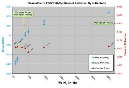 Example of Si3N4 modified stress via. varying N2 flow. Refractive index is relatively constant (one outlier), and stress varies continuously from tensile to compressive. (Demis D. John 2011, Blumenthal Group)

SiOxNy deposition (PECVD #1)
- SiOxNy Standard Recipe
- SiOxNy Data 2014 - Rate, Index etc.
- SiOxNy1000A Thickness uniformity 2014
Standard Cleaning Procedure (PECVD #1)
The cleaning procedure is very important in order to have consistent result on this tool and also to keep particulate count low. After each deposition you should clean the tool following instructions carefully. The clean is done in two steps:
- Wet cleaning (start cleaning by using a cleanroom wipe sprayed with DI. Wipe chamber sidewalls with it. Finish cleaning by using the cleanroom wipe sprayed with IPA. )
- Load the recipe for cleaning "CF4/O2 Clean" (edit the recipe and change ONLY time of cleaning). Follow instructions regarding a required time for cleaning.
| Film Dep'd | Cleaning Time |
|---|---|
| SiO2 | TBD |
| Si3N4 | TBD |
| SiOxNy | Same as XYZ |
Standard Cleaning Recipe (PECVD#1): "CF4/O2 Clean"
Click the above link for a screenshot of the standard cleaning recipe, for which you will enter a custom time. The recipe is set up so that it will pop up a window for the cleaning time upon running the recipe - you do not need to edit the recipe before running it.
PECVD 2 (Advanced Vacuum)
PECVD 2 Process Control Plots - Plots of all process control data
SiO2 deposition (PECVD #2)
- SiO2 [PECVD 2] New Standard Recipe - "STD SiO2 v2"
- SiO2 [PECVD 2] Old Standard Recipe - "STD SiO2"
- SiO2 [PECVD 2] Current Process Control Data
- SiO2 [PECVD 2] Historical Data - Before Oct. 2021
SiN deposition (PECVD #2)
- Si3N4 [PECVD 2] New Standard Recipe - "STD Si3N4 v3"
- Si3N4 [PECVD 2] Old Standard Recipe - "Nitride2"
- Si3N4 [PECVD 2] Current Process Control Data
- Si3N4 [PECVD 2] Historical Data - Before Oct. 2021
Low-Stress SiN deposition (PECVD #2)
Low-Stress Silicon Nitride, Si3N4 (< ±100 MPa)
- Low Stress Si3N4 [PECVD 2] New Standard Recipe - " STD LS-Si3N4 v4 "
- Low Stress Si3N4 [PECVD 2] Standard Recipe - " Old LSNitride2 recipe "
- Low Stress Si3N4 [PECVD 2] Current Process Control Data
- Plots of Low-Stress Si3N4 Process Control Data
- Low Stress Si3N4 [PECVD 2] Historical Data - Before Oct. 2021
- Old Versions of the recipe:
- LS Nitride2 Standard Recipe 2014-5/9/2018
- STD LSNitride2 5/9/2018
Amorphous-Si deposition (PECVD #2)
Standard Cleaning Procedure (PECVD #2)
The cleaning procedure is very important in order to have consistent result on this tool and also to keep particulate count low. After each deposition you should clean the tool following instructions carefully. The clean is done in two steps:
- (If >29min dep time) Wet cleaning: Start cleaning by using a cleanroom wipe sprayed with DI. Wipe upper chamber sidewalls with it. Finish cleaning by using the cleanroom wipe sprayed with IPA & wiping again.
- Load the recipe for cleaning "STD CF4/O2 Clean" (edit the recipe and change ONLY time of cleaning). Follow instructions regarding required time for cleaning.
Standard Clean Recipe (PECVD#2): "STD CF4/O2 Clean"
Click the above link for a screenshot of the standard cleaning recipe, for which you will enter a custom time. The recipe is set up so that it will pop up a window for the cleaning time upon running the recipe - you do not need to edit the recipe before running it.
Clean Times (PECVD#2)
| Film Deposited | Cleaning Time (Dry) |
|---|---|
| SiO2 | 1 min. clean for every 1 min. deposition |
| Si3N4 | 1 min. clean for every 7 min of deposition |
| If > 29min total dep time
(Season + Dep) |
Wet Clean the Upper Lid/Chamber
DI water then Isopropyl Alcohol on chamber wall & portholes |
ICP-PECVD (Unaxis VLR)
2020-02: New recipes have been characterized for low particulate count and repeatability. Only staff-supplied recipes are allowed in the tool. Please follow the new procedures to ensure low particle counts in the chamber.
The system currently has Deuterated Silane (SiD4) installed - identical to the regular Silicon precursor SiH4, except that it significantly lowers optical absorption in the near-infrared due to shifted molecular vibrations/molecular weights. This gas is more expensive and thus more applicable to optical application than to general-purpose SiN films.
Process Control Data (Unaxis ICP-PECVD)
- ICP-PECVD Process Control Plots - Plots of all Process Control data
- Low Deposition Rate SiO2
- High Deposition Rate SiO2
- Si3N4
- Low Stress Si3N4
Low Deposition Rate SiO2 [ICP-PECVD]
- Low Deposition Rate SiO2 [ICP-PECVD] - Standard Recipe - "SiO2 LDR250C"
- Low Deposition Rate SiO2 [ICP-PECVD] - Process Control Data
- Low Deposition Rate SiO2 [ICP-PECVD] - Historical Data - before Oct. 2021
High Deposition Rate SiO2 [ICP-PECVD]
- High Deposition Rate SiO2 [ICP-PECVD] - Standard Recipe - "SiO2 HDR250C"
- High Deposition Rate SiO2 [ICP-PECVD] - Current Process Control Data
- High Deposition Rate SiO2 [ICP-PECVD] - Historical Data
Si3N4 [ICP-PECVD]
- Si3N4 [ICP-PECVD] - Standard Recipe - "SiN 250C"
- Si3N4 [ICP-PECVD] - Current Process Control Data
- Si3N4 [ICP-PECVD] - Historical Data - before Oct. 2021
Low Stress Si3N4 [ICP-PECVD]
- Low Stress Si3N4 [ICP-PECVD] - Standard Recipe - "SiN Low Stress 250C"
Standard Cleaning Procedure [ICP-PECVD]
You must edit the Post-Dep Clean recipe to correspond to your deposited thickness and material. See the Operating Procedure on the Unaxis Tool Page for details.
- SiNx etches at 20nm/min
- SiO2 etches at 40nm/min
Standard Clean Recipe
To Be Added
General Recipe Notes (Unaxis VLR ICP-PECVD)
- RF1 = Bias
- RF2 = ICP Power
- All recipes start with an Argon pre-clean with 0W bias (gentle), to improve adhesion/nucleation.
- Maximum SiO2 Dep. thickness allowed: 800nm
- Above this thickness, you must run a chamber clean/season before depositing more onto your product wafer.