Difference between revisions of "PECVD 2 (Advanced Vacuum)"
Jump to navigation
Jump to search
| Line 28: | Line 28: | ||
== Documentation == |
== Documentation == |
||
| + | * |
||
| − | * [https://wiki.nanotech.ucsb.edu/wiki/File:Advanced_Vacuum_PECVD.pdf Operating Instructions] |
||
* [[Wafer Coating Process Traveler]] |
* [[Wafer Coating Process Traveler]] |
||
* For particle counting method, see the [[Wafer scanning process traveler|Surfscan Scanning Procedure]] |
* For particle counting method, see the [[Wafer scanning process traveler|Surfscan Scanning Procedure]] |
||
Revision as of 09:53, 27 May 2020
| |||||||||||||||||||||
About
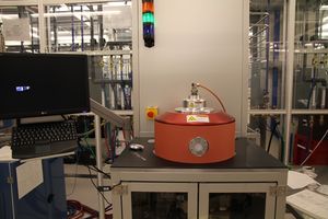
This open-load system is dedicated to PECVD of SiO2, SiNx, SiOxNy, and a-Si using Silane (2%SiH4, 98% He), N2O, NH3, and N2 gases. The sample electrode has a 270mm diameter useable area, allowing for multiple 4” wafer depositions in a single run. Standard operating temperature is 300C, but can be user changed for temps ranging anywhere from 250 to 350C. The system is equipped with a dual generator, dual frequency option for growth of low-stress Nitride films.
Recipes
- Recipes for SiO2, Si3N4 and Low-Stress Si3N4 can be found on the PECVD Recipes Page:
- A list of all available deposited films can be found on the Vacuum Deposition Recipes page:
See Also
Documentation
- Wafer Coating Process Traveler
- For particle counting method, see the Surfscan Scanning Procedure
