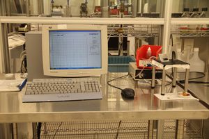
Optical Film Thickness (Filmetrics)
Jump to navigation
Jump to search
The printable version is no longer supported and may have rendering errors. Please update your browser bookmarks and please use the default browser print function instead.
|
About
This tool is for thickness and optical property measurements of films on substrates. The technique used is white light reflection. Data is taken with normal incidence reflection of white light (400 nm – 850 nm) from the surface. The data is modeled and the optical parameters are adjusted to give a best least-squared fit to the data. The accuracy of the technique will depend on the thickness of the film and the optical models used for the fitting of the data. For a more complete description go to Filmetrics.
Equipment Specifications
- 400-850 nm reflection spectrum
- 150 A to 50 um thickness only measurement
- 1000 A to 10 um thickness, n, and k measurements
- 1 nm accuracy at 500 nm thickness
- Manual wafer placement
- Data can all be saved
- Can model up to three layers
