Difference between revisions of "Optical Film Thickness & Wafer-Mapping (Filmetrics F50)"
(→Equipment Specifications: added photo, minor updates) |
(Added meas spot size) |
||
| (4 intermediate revisions by 2 users not shown) | |||
| Line 1: | Line 1: | ||
| − | {{ |
+ | {{tool2|{{PAGENAME}} |
|picture=FIlmetrics_F50_Photo_v1.jpg |
|picture=FIlmetrics_F50_Photo_v1.jpg |
||
|type = Inspection, Test and Characterization |
|type = Inspection, Test and Characterization |
||
| − | |super= |
+ | |super= Aidan Hopkins |
| + | |super2= Demis D. John |
||
|location=Bay 6 |
|location=Bay 6 |
||
|description = Thin-Film Reflectometry |
|description = Thin-Film Reflectometry |
||
|manufacturer = [http://www.filmetrics.com/ Filmetrics] |
|manufacturer = [http://www.filmetrics.com/ Filmetrics] |
||
| − | |model = F50 |
+ | |model = F50-UV |
|materials = |
|materials = |
||
}} |
}} |
||
| − | = |
+ | =About= |
This tool is for thickness and optical property measurements of films on substrates, including mapping of thin-films on full wafers. |
This tool is for thickness and optical property measurements of films on substrates, including mapping of thin-films on full wafers. |
||
| − | The technique used is white light reflection. Data is taken with normal incidence reflection of white light |
+ | The technique used is white light reflection. Data is taken with normal incidence reflection of white light from the surface using a Deuterium (UV) and Halogen (Vis-nIR) lamps. |
The motorized stage automatically acquires optical reflection spectra at programmed points across the wafer. At each point, the reflection spectrum is baselines, and the reflection data is modeled at each point, and finally the optical parameters (thickness/refractive index/absorption) are adjusted to give a best least-squared fit to the data. The accuracy of the technique will depend on the thickness of the film and the optical models used for the fitting of the data. For a more complete description go to [http://www.filmetrics.com/ Filmetrics]. |
The motorized stage automatically acquires optical reflection spectra at programmed points across the wafer. At each point, the reflection spectrum is baselines, and the reflection data is modeled at each point, and finally the optical parameters (thickness/refractive index/absorption) are adjusted to give a best least-squared fit to the data. The accuracy of the technique will depend on the thickness of the film and the optical models used for the fitting of the data. For a more complete description go to [http://www.filmetrics.com/ Filmetrics]. |
||
=Equipment Specifications= |
=Equipment Specifications= |
||
| + | |||
| − | *190- |
+ | *190-1100 nm reflection spectrum |
*Deuterium (UV) and Halogen (Vis-nIR) light sources |
*Deuterium (UV) and Halogen (Vis-nIR) light sources |
||
*10 Å to 150 µm thickness, ''n'', and ''k'' measurements |
*10 Å to 150 µm thickness, ''n'', and ''k'' measurements |
||
*Motorized mapping on wafers up to 150mm. |
*Motorized mapping on wafers up to 150mm. |
||
*Small substrates also possible, ≥ 2-3mm |
*Small substrates also possible, ≥ 2-3mm |
||
| + | *Approx. 1-2mm measurment spot size area |
||
| + | **Best for unpatterned samples. |
||
*Spectrum Data can be exported |
*Spectrum Data can be exported |
||
*Can model up to three layers with accuracy |
*Can model up to three layers with accuracy |
||
| − | = |
+ | =Operating Procedures= |
| + | |||
| − | ''To be added'' |
||
| + | *[[Filmetrics F50 - Operating Procedure|Basic Operating Procedure]] |
||
| + | *[[Filmetrics F50 - Adding a New Model|Add a Model for a New Thin-Film]] - ''To Be Added'' |
||
Latest revision as of 10:03, 13 September 2022
| ||||||||||||||||||||||||||||
About
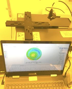
This tool is for thickness and optical property measurements of films on substrates, including mapping of thin-films on full wafers. The technique used is white light reflection. Data is taken with normal incidence reflection of white light from the surface using a Deuterium (UV) and Halogen (Vis-nIR) lamps.
The motorized stage automatically acquires optical reflection spectra at programmed points across the wafer. At each point, the reflection spectrum is baselines, and the reflection data is modeled at each point, and finally the optical parameters (thickness/refractive index/absorption) are adjusted to give a best least-squared fit to the data. The accuracy of the technique will depend on the thickness of the film and the optical models used for the fitting of the data. For a more complete description go to Filmetrics.
Equipment Specifications
- 190-1100 nm reflection spectrum
- Deuterium (UV) and Halogen (Vis-nIR) light sources
- 10 Å to 150 µm thickness, n, and k measurements
- Motorized mapping on wafers up to 150mm.
- Small substrates also possible, ≥ 2-3mm
- Approx. 1-2mm measurment spot size area
- Best for unpatterned samples.
- Spectrum Data can be exported
- Can model up to three layers with accuracy
Operating Procedures
- Basic Operating Procedure
- Add a Model for a New Thin-Film - To Be Added
