Difference between revisions of "Molecular Vapor Deposition"
Jump to navigation
Jump to search
(link to nanoimprint FDTS recipe) |
|||
| (8 intermediate revisions by 3 users not shown) | |||
| Line 1: | Line 1: | ||
| − | {{ |
+ | {{tool2|{{PAGENAME}} |
|picture=MVD.jpg |
|picture=MVD.jpg |
||
|type = Vacuum Deposition |
|type = Vacuum Deposition |
||
| − | |super= |
+ | |super= Lee Sawyer |
| + | |super2= Aidan Hopkins |
||
| − | |phone=(805) |
+ | |phone=(805) 893-2123 |
|location=Bay 4 |
|location=Bay 4 |
||
| − | |email= |
+ | |email=lee_sawyer@ucsb.edu |
|description = Molecular Vapor Deposition System |
|description = Molecular Vapor Deposition System |
||
|manufacturer = [http://www.appliedmst.com/ Applied Microstructures Inc.] |
|manufacturer = [http://www.appliedmst.com/ Applied Microstructures Inc.] |
||
|materials = |
|materials = |
||
}} |
}} |
||
| − | = |
+ | ==About== |
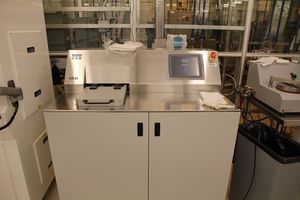
The Molecular Vapor deposition system is used for deposition of a monolayer-thick fluorocarbon film for producing extremely hydrophobic surfaces used for anti-sticking layers for nanoimprinting or anti-stiction layers for MEMS. The system has integrated Oxygen plasma cleaning for organic removal and surface activation and can be run at temperatures up to 80°C. Multi-step recipes can be created. The system is currently configured for FDTS (perflourodecyltricholorsilane) and water to producing the coatings. Up to 6” wafers can be coated in the system. |
The Molecular Vapor deposition system is used for deposition of a monolayer-thick fluorocarbon film for producing extremely hydrophobic surfaces used for anti-sticking layers for nanoimprinting or anti-stiction layers for MEMS. The system has integrated Oxygen plasma cleaning for organic removal and surface activation and can be run at temperatures up to 80°C. Multi-step recipes can be created. The system is currently configured for FDTS (perflourodecyltricholorsilane) and water to producing the coatings. Up to 6” wafers can be coated in the system. |
||
| − | == |
+ | ==Recipes== |
| + | |||
| − | * |
+ | *[https://wiki.nanotech.ucsb.edu/w/index.php?title=Lithography_Recipes#Nanoimprinting_Recipes Nanoimprinting recipes] using FDTS non-stick layer |
| + | *[https://signupmonkey.ece.ucsb.edu/wiki/images/3/3c/MVD_Standard_Recipes.pdf MVD Standard Recipes] |
||
| + | |||
| + | ==Documentation== |
||
| + | |||
| + | *[https://signupmonkey.ece.ucsb.edu/wiki/images/f/f4/MVD_SOP.pdf MVD Standard Operating Procedure] |
||
| + | *[[MVD - Wafer Coating - Process Traveler|Wafer Coating - Process Traveler]] |
||
Latest revision as of 10:34, 30 August 2022
| ||||||||||||||||||||||||||
About
The Molecular Vapor deposition system is used for deposition of a monolayer-thick fluorocarbon film for producing extremely hydrophobic surfaces used for anti-sticking layers for nanoimprinting or anti-stiction layers for MEMS. The system has integrated Oxygen plasma cleaning for organic removal and surface activation and can be run at temperatures up to 80°C. Multi-step recipes can be created. The system is currently configured for FDTS (perflourodecyltricholorsilane) and water to producing the coatings. Up to 6” wafers can be coated in the system.
Recipes
- Nanoimprinting recipes using FDTS non-stick layer
- MVD Standard Recipes
