Difference between revisions of "Lift-Off with DUV Imaging + PMGI Underlayer"
(Text replacement - "/wiki/index.php/" to "/wiki/index.php?title=") |
(→Process Limits: suggest LOL, PMGI double-spin etc.) |
||
| (One intermediate revision by one other user not shown) | |||
| Line 5: | Line 5: | ||
==Tips== |
==Tips== |
||
| − | Please see our [[https://wiki.nanotech.ucsb.edu/ |
+ | Please see our [[https://wiki.nanotech.ucsb.edu/w/index.php?title=Lithography_Recipes#Lift-Off_Techniques Bi-Layer Lift-Off Tutorial]] to understand the limitations and requirements for good lift-off. |
*Remember that gaps in between adjacent metal traces can lift-off during the develop! |
*Remember that gaps in between adjacent metal traces can lift-off during the develop! |
||
| Line 17: | Line 17: | ||
*Make sure to use a vertical evaporation - EBeam4 or EBeam1. EBeam3 is not vertical unless special care is taken. |
*Make sure to use a vertical evaporation - EBeam4 or EBeam1. EBeam3 is not vertical unless special care is taken. |
||
| − | === |
+ | ===Process Limits=== |
This process is written with PMGI SF-5 @ 4krpm, which spins to about 130nm |
This process is written with PMGI SF-5 @ 4krpm, which spins to about 130nm |
||
| + | |||
| − | * <u>Maximum metal thickness</u> = 130nm/2 ≈ 6'''5nm''' |
||
| − | * |
+ | *<u>Maximum metal thickness</u> = 130nm/2 ≈ 6'''5nm''' |
| + | *Undercuts laterally about 130-140nm, so <u>minimum gap between metals</u> = (2 x 140nm) + ~30nm ≈ '''350nm''' |
||
| + | |||
Adjust the PMGI layer thickness to adjust these process limits. |
Adjust the PMGI layer thickness to adjust these process limits. |
||
| + | |||
| + | PMGI could be spun thicker, or double-spun to get thicker underlayers (develop time & undercut will increase accordingly). |
||
| + | |||
| + | PMGI underlayer could be replaced with LOL1000/LOL2000, or another developable underlayer. |
||
==Suggested Process for Liftoff== |
==Suggested Process for Liftoff== |
||
| Line 36: | Line 42: | ||
| |
| |
||
|- |
|- |
||
| − | |PMGI-Bake: 220°C, 3min (BrewerSci lift-pin hotplate). |
+ | |PMGI-Bake: 220°C, 3min (BrewerSci lift-pin hotplate). |
|Can just place wafer directly onto hotplate surface. |
|Can just place wafer directly onto hotplate surface. |
||
Optionally can use lift-pins & Recipe "'''00 220deg, 3min Vac'''"; |
Optionally can use lift-pins & Recipe "'''00 220deg, 3min Vac'''"; |
||
Revision as of 11:21, 28 October 2021
Developed by Demis D. John, ~2017-2019
This process is intended for Deep-UV Exposure on the ASML DUV Stepper. PMGI is used as the underlayer, which is exposed at the same time as the imaging resist.
Adjust spin speed or switch to a different PMGI formulation to tailor the underlayer thickness to your desired metal thickness.
Tips
Please see our [Bi-Layer Lift-Off Tutorial] to understand the limitations and requirements for good lift-off.
- Remember that gaps in between adjacent metal traces can lift-off during the develop!
- Need underlayer thickness approx. 2x the desired metal thickness.
- The underlayer will develop laterally from both sides which can lift-off the imaging resist, so:
- Minimum gap between adjacent metals should then be: less than 0.5 * underlayer thickness
- Want at least 30-50nm of underlayer width left to support the imaging resist, so the PR doesn't fall over/collapse.
- Make sure to use a vertical evaporation - EBeam4 or EBeam1. EBeam3 is not vertical unless special care is taken.
Process Limits
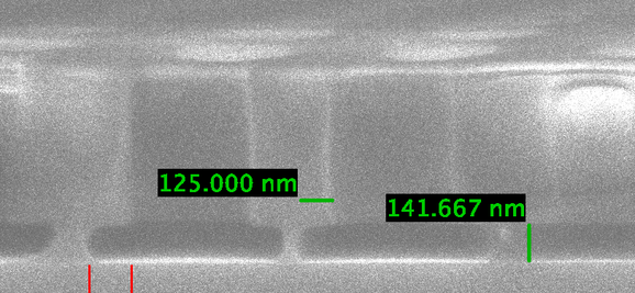
This process is written with PMGI SF-5 @ 4krpm, which spins to about 130nm
- Maximum metal thickness = 130nm/2 ≈ 65nm
- Undercuts laterally about 130-140nm, so minimum gap between metals = (2 x 140nm) + ~30nm ≈ 350nm
Adjust the PMGI layer thickness to adjust these process limits.
PMGI could be spun thicker, or double-spun to get thicker underlayers (develop time & undercut will increase accordingly).
PMGI underlayer could be replaced with LOL1000/LOL2000, or another developable underlayer.
Suggested Process for Liftoff
| De-H2O Bake (eg. 220°C, 1m+)
- or - Technics O2 ash (300mT, 100W), 15sec |
Oxygen ash is faster and more effective |
| Spin PMGI SF-5 @ 4krpm (rcp 7) | |
| POLOS underside clean: 2000rpm, ACE/ISO/N2 | |
| PMGI-Bake: 220°C, 3min (BrewerSci lift-pin hotplate). | Can just place wafer directly onto hotplate surface.
Optionally can use lift-pins & Recipe "00 220deg, 3min Vac"; --> To prevent wafer sliding: Enable Vacuum with overhead valve, only for wafer landing and then turn off. |
| Spin UV-6-0.8 @ rcp 6 (3.5krpm) | |
| POLOS underside clean: 2000rpm, ACE/ISO/N2 | |
| Soft-Bake = 135°C, 1min (builtin hotplate) | |
| (check underside for particulates) | |
| ASML Exposure | |
| Default: Exp = 37.5mJ // foc = –0.10 | Try this exposure dose but might need to do a FocArray (smaller Image Distribution eg. 5x5) to find proper exposure. |
| PEB = 135°C, 1.5min (built-in hotplate) | |
| Dev (300MiF) = 50sec (CRITICAL time) | Use cassette & H2O rinse dish prepared
--> not stirring, instead very slow/gentle lift/drop at various angles or gentle swish just to mix developer slightly. |
| DI rinse | Very Gently! Dunk into prepared DI dish, and dump/fill gently 2x. Don’t allow direct hard water to hit PR surface. |
| PEii Technics O2: 30sec (100W/300mT) | May increase feature size openings by ~50nm. |
| Metal Evaporation
(insert steps) |
EBeam#4 or EBeam#1 with vertical/4-inch holders (not planetary) |
| Lift-off in NMP | Facing down or vertical.
Optional: going directly into continuous Ultrasonic can reduce residual particles. |
Data
• For PMGI Baked at 220°C for 3min, the PMGI dissolves in AZ 300MIF at a rate of approximately ~600nm/min.
Images / Examples
