Difference between revisions of "IR Aligner (SUSS MJB-3 IR)"
Jump to navigation
Jump to search
(System information) |
(SOP rev) |
||
| Line 40: | Line 40: | ||
*[https://wiki.nanotech.ucsb.edu/wiki/images/d/de/MJB_3_SOP.pdf MJB 3 Standard Operating Procedure] |
*[https://wiki.nanotech.ucsb.edu/wiki/images/d/de/MJB_3_SOP.pdf MJB 3 Standard Operating Procedure] |
||
*[https://wiki.nanotech.ucsb.edu/w/images/1/11/MJB_3_IR_Alignment_Mode_Conversion.pdf MJB 3 IR Alignment Mode Conversion Procedure] |
*[https://wiki.nanotech.ucsb.edu/w/images/1/11/MJB_3_IR_Alignment_Mode_Conversion.pdf MJB 3 IR Alignment Mode Conversion Procedure] |
||
| − | *[https://wiki.nanotech.ucsb.edu/w/images/ |
+ | *[https://wiki.nanotech.ucsb.edu/w/images/7/70/MJB_3_IR_Camera_SOP_Rev_B.pdf MJB 3 IR Camera Operating Procedure] |
Latest revision as of 11:56, 7 August 2020
|
About
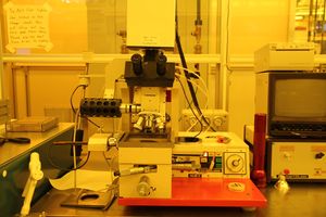
This is a high-performance contact mask aligner with backside alignment capability for opaque materials using IR. It is a versatile, user-friendly compact unit that has a foot print of 600 x 800 mm². The resolution (depending on contact mode, optics and exposure wavelength and "operator technique") is down to 1 micron (hard contact). The aligner is configured for the near-UV window (365 and 405 nm). Exposures can be done on substrates from small "piece parts" of less than 1 cm square to substrates of 3 inch diameter or square. Masks up to 4 inches in size can be used although patterns should be well away from the mask plate edges due to the fact such plates can only be shifted a limited distance in the x and y.
Detailed Specifications
- Wafer size: 3" max. for vacuum mode; 4” for soft contact (3” x 3” exposure area)
- Substrate size: 3" x 3" max.
- Wafer / substrate thickness: 0-4.5 mm
- Exposure optics:
- 280-450 nm/200 W mercury lamp (can filter to 350 nm)
- Uniformity:
- ±3% over 2" diameter
- ±5% over 3" diameter
Special Notes / Additional Comments
- 200 W mercury lamp
- Top side alignment (visible) can be performed on this aligner as well with a quick tooling change
- Infrared Transmission Alignment System:
- Motor positioned IR light source under chuck
- Special glass chucks transparent to IR but opaque to UV and visible light
- In-line video camera/monitor for substrate backside viewing and alignment to front-side
- This aligner does not support vacuum contact mode
- For processes using this tool please go to the contact lithography process page
