Difference between revisions of "ICP Etching Recipes"
(→Through Silicon Via (TSV) etch (DSEiii): no-wax proces sis acceptable) |
|||
| (325 intermediate revisions by 6 users not shown) | |||
| Line 1: | Line 1: | ||
{{recipes|Dry Etching}} |
{{recipes|Dry Etching}} |
||
| + | |||
| − | =[[ICP Etch 1 (Panasonic E626I)]]= |
||
| + | =[[DSEIII_(PlasmaTherm/Deep_Silicon_Etcher)]]= |
||
| + | |||
| + | ==Process Control Data (DSEiii)== |
||
| + | |||
| + | *'''''[[To Be Added]]''''' |
||
| + | |||
| + | ==Edge-Bead Removal (DSEiii)== |
||
| + | Make sure to remove photoresist from edges of wafer, or PR may stick to the top-side wafer clamp and destroy your wafer during unload! |
||
| + | |||
| + | *[[ASML DUV: Edge Bead Removal via Photolithography|Edge Bead Removal via Photolithography]]: use a custom metal mask to pattern the photoresist with a flood exposure. |
||
| + | **If you are etching fully through a wafer, remember that removal of edge-bead will cause full etching in the exposed areas. To prevent a wafer from falling into the machine after the etch, you can [[Packaging Recipes#Wafer Bonder .28Logitech WBS7.29|mount to a carrier wafer using wax]]. |
||
| + | *[[Photolithography - Manual Edge-Bead Removal Techniques|Manual PR Edge-Bead Removal]] - using swabs and EBR100. This is prone to error and easy to accidentally leave a blob of PR on the edge - so be extra careful to ensure NO PR is left on the edges! |
||
| + | |||
| + | ==High Rate Bosch Etch (DSEIII)== |
||
| + | |||
| + | *[//wiki.nanotech.ucsb.edu/wiki/images/4/4a/10-Si_Etch_Bosch_DSEIII.pdf Bosch Process Recipe and Characterization] - Standard recipe on the tool. |
||
| + | **Recipe Name: "'''''Plasma-Therm Standard DSE'''''" (''Production'' - copy to your ''Personal'' category) |
||
| + | **Standard [https://en.wikipedia.org/wiki/Deep_reactive-ion_etching#Bosch_process Bosch Process] for high aspect-ratio, high-selectivity Silicon etching. |
||
| + | **Cycles between polymer deposition "Dep" / Polymer etch "Etch A" / Si etch "Etch B" steps. Step Times gives fine control. |
||
| + | ***To reduce roughening/grassing (black silicon), reduce Dep step time by ~20%. |
||
| + | **Patterns with different exposed/etched areas will have different "optimal" parameters. |
||
| + | **Approx Selectivity to Photoresist: ~80 or better. |
||
| + | ***Larger open area, lower selectivity and lower etch rate. |
||
| + | ***Thick PR's approx ≥10µm tend to burn, avoid thick PR's. They also make edge-bead removal very difficult. |
||
| + | **Selectivity to SiO2 should be higher, not yet measured. |
||
| + | **Selectivity to Al<sub>2</sub>O<sub>3</sub> is extremely high, >9000. See below TSV process for processing notes on this film. |
||
| + | **If you need to pattern all the way to the edge of the wafer, PR won't work because you have to remove the edge-bead of photoresist (see above). Instead use hardmask process (See "Through Silicon Via" etch below). |
||
| + | |||
| + | ::[[File:DSEiii Bosch Ecth SEM Example 01.png|alt=Example SEM image|none|thumb|465x465px|Example of 100µm Deep Bosch Etched Silicon posts with hard mask. Close inspection shows the horizontal "scalloping" from the cycling nature of the etch. (Image Credit: Demis D. John, 2021-07)]] |
||
| + | |||
| + | ===Through Silicon Via (TSV) etch (DSEiii)=== |
||
| + | Since the topside clamp requires the removal of photoresist on the outermost ~5-7mm of the wafer, this makes PR incompatible with through-silicon etching (as the outer edges would be etched-through, dropping the inner portion into the chamber). In addition, in practice we have found that thick PR often roughens and burns during long ~30-60min etches, making removal very difficult. |
||
| + | |||
| + | Instead, we recommend the following process with Al<sub>2</sub>O<sub>3</sub> hardmask: |
||
| + | <big>'''NOTE''': We have recently found that the wax-mounting process process can leave wax on the wafer clamp, causing the next user's wafer to get stuck and fail transfer! '''<u>DO NOT RUN</u>''' the wax-mounting process without discussing with staff first. ''(Through-wafer process with no wax is still acceptable.)'' -- [[Demis D. John|Demis]] 2024-03-11</big> |
||
| + | {| class="wikitable" |
||
| + | ! colspan="2" |Process for Through-Wafer Silicon Etching |
||
| + | |- |
||
| + | |Process to etch through ~550µm Silicon |
||
| + | |''<small>[[Demis D. John]] & [[Biljana Stamenic]] 2022-11-11. Please consider our [[Frequently Asked Questions#Publications acknowledging the Nanofab|publication policy]] if you use/modify this process.</small>'' |
||
| + | |- |
||
| + | |Deposit 150nm Al<sub>2</sub>O<sub>3</sub> on either: |
||
| + | |||
| + | *[https://wiki.nanotech.ucsb.edu/w/index.php?title=Sputtering_Recipes#Al2O3_deposition_.28IBD.29 Veeco Nexus IBD] |
||
| + | *AJA Sputter [https://wiki.nanotech.ucsb.edu/wiki/Sputtering_Recipes#Materials_Table_.28Sputter_3.29 3]/[https://wiki.nanotech.ucsb.edu/wiki/Sputtering_Recipes#Al2O3_Deposition_.28Sputter_4.29 4]/[https://wiki.nanotech.ucsb.edu/wiki/Sputtering_Recipes#Materials_Table_.28Sputter_5.29 5] (Check which has Al target installed) |
||
| + | |May need to do dep. rate check beforehand. |
||
| + | |- |
||
| + | |Deposit ~3nm SiO<sub>2</sub>, ''in situ'' (same machine as above) |
||
| + | |This improves adhesion to photoresist and prevents developer attacking the Al<sub>2</sub>O<sub>3</sub>. |
||
| + | |- |
||
| + | |Lithography - your preferred method. Needs approx. ≥500nm thick PR. |
||
| + | | |
||
| + | |- |
||
| + | |Etch the [https://wiki.nanotech.ucsb.edu/w/index.php?title=ICP_Etching_Recipes#Al2O3_Etching_.28Panasonic_2.29 Al2O3 in Panasonic ICP 1/2] |
||
| + | |Use 50W version. Overetch by ~20%, will also etch through the thin SiO<sub>2</sub> layer. |
||
| + | |- |
||
| + | |Strip PR - either ''[https://wiki.nanotech.ucsb.edu/w/index.php?title=ICP_Etching_Recipes#Photoresist_Etch.2FStrip_.28Panasonic_2.29 in situ]'', or via NMP 80°C soak followed by [https://wiki.nanotech.ucsb.edu/wiki/Oxygen_Plasma_System_Recipes#Ashers_.28Technics_PEII.29 PEii Technics ashing]. |
||
| + | |''In situ'' PR strip appears to give better + faster results. |
||
| + | |- |
||
| + | |If pieces of the wafer are at risk of falling into the chamber, mount the product wafer to a carrier wafer: |
||
| + | [https://wiki.nanotech.ucsb.edu/wiki/Logitech_WBS7_-_Procedure_for_Wax_Mounting_with_bulk_Crystalbond_Stick Logitech Wax Mounting Recipe - Bulk Crystal Bond] |
||
| + | |||
| + | |||
| + | If you are only etching small holes through the wafer (majority of wafer is intact), then wax-mounting is not necessary. |
||
| + | |Critical - Ensure no wax is present on either side or edge of wafer prior to DSE etching, or wafer may break in the DSE during robot unload! |
||
| + | |- |
||
| + | |Use POLOS spinners with ACE/ISO to clean front and back of wafer. |
||
| + | '''''IMPORTANT''''' for wax-mounting, to ensure wax does not stick your wafer to the DSE clamp. |
||
| + | |||
| + | Observe ''carefully'' for any wax protruding from between wafers - redo spin-clean as needed. |
||
| + | |Also make sure wax thickness is not too thick, of long etches could cause wax to seep out from between the wafers. |
||
| + | |- |
||
| + | |DSEiii etch - reduce Dep step to eliminate grassing: |
||
| + | |||
| + | *Bosch Cycles: Dep: 1.2sec / Etch A: 1.5sec / Etch B: 2.0sec |
||
| + | *Rate ≈ 4.25µm / min |
||
| + | |Can use Lasermonitor and/or Camera to observe when etch is fully through. Trenches may get black/rough, but then clear up when fully etched. |
||
| + | Record Helium FLOW during recipe run, for next step (if He leaks). |
||
| + | |||
| + | Ok to remove wafer, observe/measure, and re-load for etching. |
||
| + | |||
| + | If see black grass and etch rate drops, may need to run an O2 plasma with [[Ashers (Technics PEII)|Technics PEii]] few min to remove polymer, reduce Dep step time and then continue. |
||
| + | |- |
||
| + | |If you did not wax-mount your wafer, the recipe will eventually fail for Helium Pressure/Flow our of compliance. This is because the cooling Helium leaks through the wafer when the openings get fully etched through. |
||
| + | Once this happens, |
||
| + | |||
| + | *Leave your wafer in the chamber, then |
||
| + | |||
| + | *Edit recipe to set Helium Cooling (first step only) to "Flow Control Only". Choose typical flow of normal process from above (Something like ~6sccm? Not sure.) |
||
| + | | |
||
| + | |- |
||
| + | |Strip Al<sub>2</sub>O<sub>3</sub>/SiO<sub>2</sub> either with HF, or same Pan1/2 dry etch as above. |
||
| + | | |
||
| + | |- |
||
| + | |IF wax-mounted - either |
||
| + | |||
| + | *dissolve in Acetone overnight (make sure to excess-fill enough and cover tightly with tinfoil so it doesn't dry up), complete with ACE/ISO rinse |
||
| + | |||
| + | OR |
||
| + | |||
| + | *place wafer on tinfoil-covered hotplate at 150°C, and slide product wafer off, then |
||
| + | **ACE/ISO clean to remove wax. |
||
| + | | |
||
| + | |- |
||
| + | | colspan="2" |''<small>If you '''publish''' using the above process, please consider our [[Frequently Asked Questions#Publications acknowledging the Nanofab|publication policy]]. This process was developed by [[Biljana Stamenic]] and [[Demis D. John]], 2022.</small>'' |
||
| + | |} |
||
| + | |||
| + | ==Single-Step Low Etch Rate Smooth Sidewall Process (DSEIII)== |
||
| + | |||
| + | *[//wiki.nanotech.ucsb.edu/wiki/images/8/8f/10-Si_Etch_Single_Step_Smooth_Sidewall_DSEIII.pdf Single Step Silicon Etch Recipe and Characterization] |
||
| + | **Recipe Name: "'''''Nano Trench Etch'''''" (''Production'' - copy to your ''Personal'' category) |
||
| + | **Used instead of Bosch Process, to avoid scalloping on the sidewall. |
||
| + | **Lower selectivity, lower etch rate, smoother sidewalls. |
||
| + | |||
| + | =[[Fluorine ICP Etcher (PlasmaTherm/SLR Fluorine ICP)|PlasmaTherm/SLR Fluorine Etcher]]= |
||
| + | |||
| + | ===Recipe Tips=== |
||
| + | |||
| + | *RF1: Bias Power (with DCV readback) |
||
| + | *RF2: ICP Power |
||
| + | *For trouble igniting ICP plasma, add 15 to 75 W of bias power during ignition step. Typical ignition pressures 5 to 10 mT. |
||
| + | |||
| + | ==Process Control Data (Fluorine ICP Etcher)== |
||
| + | |||
| + | ===SiO<sub>2</sub> Etching with CHF3/CF4 (Fluorine ICP Etcher)=== |
||
| + | |||
| + | *[https://docs.google.com/spreadsheets/d/15hYkCqL3UNNayt4sXrvVi4mBj-OSdnF7PE29mQW9AEY/edit?usp=sharing SiO<sub>2</sub> Etching with CHF3/CF4 - '''Etch Data'''] |
||
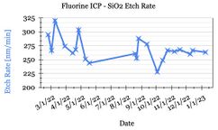
| + | *[https://docs.google.com/spreadsheets/d/15hYkCqL3UNNayt4sXrvVi4mBj-OSdnF7PE29mQW9AEY/edit#gid=1804752281 SiO<sub>2</sub> Etching with CHF3/CF4 - '''Plots'''][[File:FL-ICP Process Control Data Example.jpg|alt=example of Process Control Charts|none|thumb|242x242px|[https://docs.google.com/spreadsheets/d/15hYkCqL3UNNayt4sXrvVi4mBj-OSdnF7PE29mQW9AEY/edit#gid=1804752281 Click for Process Control Charts]|link=https://docs.google.com/spreadsheets/d/15hYkCqL3UNNayt4sXrvVi4mBj-OSdnF7PE29mQW9AEY/edit#gid=1804752281]] |
||
| + | |||
| + | ==Si Etching (Fluorine ICP Etcher)== |
||
| + | |||
| + | *[//wiki.nanotech.ucsb.edu/wiki/images/b/b8/SLR_-_SiVertHF.pdf SiVertHF] - Si Vertical Etch using C<sub>4</sub>F<sub>8</sub>/SF<sub>6</sub>/CF<sub>4</sub> and resist mask |
||
| + | **Etch Rates: Si ≈ 300-350 nm/min; SiO<sub>2</sub> ≈ 30-35 nm/min |
||
| + | **89-90 degree etch angle, ie, vertical. |
||
| + | **High selectivity to Al2O3 masks. |
||
| + | ***For high aspect ratio Si etching, try [[Atomic Layer Deposition (Oxford FlexAL)|ALD]] [[Atomic Layer Deposition Recipes#Al2O3 deposition .28ALD CHAMBER 3.29|Al<sub>2</sub>O<sub>3</sub>]] (~20-30nm) + [[Atomic Layer Deposition Recipes#SiO2 deposition .28ALD CHAMBER 3.29|SiO<sub>2</sub>]] (2nm, for PR adhesion) hardmasks followed by [https://wiki.nanotech.ucsb.edu/w/index.php?title=ICP_Etching_Recipes#Al2O3_Etching_.28Panasonic_2.29 Pan2 Al<sub>2</sub>O<sub>3</sub> etch] (will go straight through the thin SiO<sub>2</sub> without additional etch time). Works well for allowing thin PR's (eg. [[Stepper 3 (ASML)|DUV]] or [[E-Beam Lithography System (JEOL JBX-6300FS)|EBL]] PR's) to enable deep etches. |
||
| + | |||
| + | ===Process Notes/Observations=== |
||
| + | |||
| + | *Due to high selectivity against SiO2, it may be necessary to run a ~10sec 50W SiO<sub>2</sub> etch (below) to remove native oxide on Si. This can be performed ''in situ'' before the Si etch. |
||
| + | *We have observed that full-wafers with small open area in ''photoresist masks'' might require a recalibration of the C4F8/SF6 ratio in order to prevent very low etch rates. |
||
| + | |||
| + | ==SiO2 Etching (Fluorine ICP Etcher)== |
||
| + | |||
| + | *[//wiki.nanotech.ucsb.edu/w/images/f/f6/SiO2_Etch%2C_Ru_HardMask_-_Fluorine_ICP_Etch_Process_-_Ning_Cao_2019-06.pdf SiO2 Etching using Ruthenium Hardmask] - Full Process Traveler |
||
| + | **''Ning Cao & Bill Mitchell, 2019-06'' |
||
| + | **''High-selectivity and deep etching using sputtered Ru hardmask and I-Line litho.'' |
||
| + | **''Etch also works well with PR masking'' |
||
| + | **''Chemistry: CHF3/CF4'' |
||
| + | **''Variations in SiO<sub>2</sub> etch Bias Power: 50 / 200 / 400W bias.'' |
||
| + | **Ru etch selectivity to PR: 0.18 (less than 1): 150nm Ru / 800nm PR |
||
| + | **50W Bias: ('''recommended''') |
||
| + | ***Selectivity to photoresist: 1.10–1.20 |
||
| + | ***SiO<sub>2</sub> selectivity to Ru: 36 |
||
| + | ***SiO<sub>2</sub> etch rate: 263nm/min |
||
| + | **200W Bias: |
||
| + | ***SiO<sub>2</sub> selectivity to Ru: 38 |
||
| + | ***SiO<sub>2</sub> etch rate: 471nm/min |
||
| + | **This etch is detailed in the following article: [[Template:Publications#Highly Selective and Vertical Etch of Silicon Dioxide using Ruthenium Films as an Etch Mask|W.J. Mitchell ''et al.'', JVST-A, May 2021]] |
||
| + | |||
| + | ==Si<sub>3</sub>N<sub>4</sub> Etching (Fluorine ICP Etcher)== |
||
| + | <code>Developed by Bill Mitchell. Please see [[Frequently Asked Questions#Publications acknowledging the Nanofab|publication policy]].</code> |
||
| + | |||
| + | *ICP = 950/75W |
||
| + | *Pressure = 5mT |
||
| + | *Low Polymer Dep: CF4 = 60sccm |
||
| + | **Etch Rate = 420nm/min (PECVD Si<sub>3</sub>N<sub>4</sub>) |
||
| + | *Higher verticality: CF4 = 35 / CHF3 = 25 sccm |
||
| + | **Etch Rate = 380nm/min (PECVD Si<sub>3</sub>N<sub>4</sub>) |
||
| + | |||
| + | ==Photoresist & ARC (Fluorine ICP Etcher)== |
||
| + | Chain multiple Recipes in a Flow, to allow you to to do ''in situ'' BARC etching, and follow up with ''in situ'' Photoresist Strip. |
||
| + | |||
| + | ===PR/BARC Etch (Fluorine ICP Etcher)=== |
||
| + | |||
| + | *Etching [[Stepper Recipes#DUV-42P|DUV42P-6]] Bottom Anti-Reflection Coating |
||
| + | **~60nm thick (2500krpm) |
||
| + | **O2=20sccm / 10mT / RF1(bias)=100W / RF2(icp)=0W |
||
| + | **1min |
||
| + | |||
| + | ===Photoresist Strip/Polymer Removal (Fluorine ICP Etcher)=== |
||
| + | |||
| + | **O2=100sccm / 5mT / RF1(bias)=10W / RF2(icp)=825W |
||
| + | **75W Bias can be helpful for difficult to remove polymers, eg. 2min |
||
| + | **Use laser monitor to check for complete removal, overetch to remove Fluorocarbon polymers. |
||
| + | |||
| + | ==Cleaning Procedures (Fluorine ICP Etcher)== |
||
| + | ''To Be Added'' |
||
| + | |||
| + | =[[ICP Etch 1 (Panasonic E646V)]]= |
||
| + | |||
| + | ==Process Control Data (Panasonic 1)== |
||
| + | |||
| + | ===SiO<sub>2</sub> Etch with CHF<sub>3</sub>/CF<sub>4</sub> - Process Control Data (Panasonic 1)=== |
||
| + | |||
| + | *[https://docs.google.com/spreadsheets/d/1gBqCYXSl7IqpNL-yI11cuURlfZpTWwXUVM9hY_gGpT8/edit?usp=sharing SiO<sub>2</sub> Etch with CHF<sub>3</sub>/CF<sub>4</sub> - '''Etch Data'''] |
||
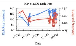
| + | *[https://docs.google.com/spreadsheets/d/1gBqCYXSl7IqpNL-yI11cuURlfZpTWwXUVM9hY_gGpT8/edit#gid=1804752281 SiO<sub>2</sub> Etch with CHF<sub>3</sub>/CF<sub>4</sub> - '''Plots'''][[File:ICP1 Process Control Data Example.jpg|alt=example chart of ICP1 SiO2 Process Control Chart|none|thumb|250x250px|[https://docs.google.com/spreadsheets/d/1gBqCYXSl7IqpNL-yI11cuURlfZpTWwXUVM9hY_gGpT8/edit#gid=1804752281 Click for Process Control Charts]|link=https://docs.google.com/spreadsheets/d/1gBqCYXSl7IqpNL-yI11cuURlfZpTWwXUVM9hY_gGpT8/edit#gid=1804752281]] |
||
| + | |||
==SiO<sub>2</sub> Etching (Panasonic 1)== |
==SiO<sub>2</sub> Etching (Panasonic 1)== |
||
| + | |||
| − | *[[media:Panasonic1-SiO-Etch.pdf|SiO<sub>2</sub> Vertical Etch Recipe]] |
||
| + | ===Recipes=== |
||
| − | *[[media:Panasonic1-SiO2-Data-Process-Variation-CHF3-revA.pdf|SiO<sub>2</sub> CHF3 Etch Variations]] |
||
| + | |||
| + | *[//wiki.nanotech.ucsb.edu/wiki/images/3/3e/Panasonic1-SiO-Etch.pdf SiO<sub>2</sub> Vertical Etch Recipe Parameters - CHF<sub>3</sub> "SiOVert"] |
||
| + | **Etch rate ≈ 2300Å/min (users must calibrate) |
||
| + | **Selectivity (SiO2:Photoresist) ≈ greater than 1:1 (users must calibrate) |
||
| + | |||
| + | ===Recipe Variations=== |
||
| + | ''Use these to determine how each etch parameter affects the process.'' |
||
| + | |||
| + | *[//wiki.nanotech.ucsb.edu/wiki/images/5/5e/Panasonic1-SiO2-Data-Process-Variation-CHF3-revA.pdf SiO<sub>2</sub> CHF<sub>3</sub> Etch Variations] - CHF3 with varying Bias and Pressure, Slanted SiO2 etching |
||
| + | |||
| + | ==SiN<sub>x</sub> Etching (Panasonic 1)== |
||
| + | |||
| + | *[//wiki.nanotech.ucsb.edu/wiki/images/c/ce/Panasonic1-SiN-Etch-Plasma-CF4-O2-ICP-revA.pdf SiN<sub>x</sub> Etch Rates and Variations - CF<sub>4</sub>-O<sub>2</sub>] |
||
| + | |||
| + | ==Al Etch (Panasonic 1)== |
||
| + | |||
| + | *[https://wiki.nanotech.ucsb.edu/wiki/images/3/3b/Panasonic-1-Al-Etch-RevA.pdf Al Etch Recipes - Cl<sub>2</sub>BCl<sub>3</sub>] |
||
| + | *[https://wiki.nanotech.ucsb.edu/wiki/images/6/60/32-Reducing_AlCl3_Corrosion_with_CHF3_plasma.pdf AlCl<sub>3</sub> Erosion Issue and the Solution] |
||
==Cr Etch (Panasonic 1)== |
==Cr Etch (Panasonic 1)== |
||
| − | *[[media:Panasonic-1-Cr-Etch-revA.pdf|Cr Etch Recipes]] |
||
| + | *[//wiki.nanotech.ucsb.edu/wiki/images/8/88/Panasonic-1-Cr-Etch-revA.pdf Cr Etch Recipes - Cl<sub>2</sub>O<sub>2</sub>] |
||
| − | =[[ICP Etch 2 (Panasonic E640)]]= |
||
| + | |||
| + | ==Ta Etch (Panasonic 1)== |
||
| + | |||
| + | *[//wiki.nanotech.ucsb.edu/wiki/images/f/f2/104_Ta_Etch.pdf Ta Etch Recipe] - Cl2/BCl3 |
||
| + | |||
| + | ==Ti Etch (Panasonic 1)== |
||
| + | |||
| + | *[//wiki.nanotech.ucsb.edu/wiki/images/4/47/Panasonic-1-Ti-Etch-Deep-RevA.pdf Ti Deep Etch Recipes - Cl<sub>2</sub>Ar] |
||
| + | **See [[doi:10.1149/1.2006647|E. Parker, ''et. al.'' Jnl. Electrochem. Soc., 152 (10) C675-C683 2005]]. |
||
| + | |||
| + | ==W-TiW Etch (Panasonic 1)== |
||
| + | |||
| + | *[//wiki.nanotech.ucsb.edu/wiki/images/7/76/Panasonic1-TiW-W-Etch-Plasma-RIE-RevA.pdf Ti-TiW Etch Recipes - SF<sub>6</sub>Ar] |
||
| + | |||
| + | ==GaAs-AlGaAs Etch (Panasonic 1)== |
||
| + | |||
| + | *[//wiki.nanotech.ucsb.edu/wiki/images/b/bb/Panasonic1-GaAs-PhotonicCrystal-RIE-Plasma-Nanoscale-Etch-RevA.pdf GaAs-Nanoscale Etch Recipe - PR mask - Cl<sub>2</sub>-BCl<sub>3</sub>-Ar] |
||
| + | *[//wiki.nanotech.ucsb.edu/wiki/images/2/26/12-Plasma_Etching_of_AlGaAs-Panasonic_ICP-1-Etcher.pdf AlGaAs Etch Recipes - Cl<sub>2</sub>N<sub>2</sub>] |
||
| + | *[//wiki.nanotech.ucsb.edu/wiki/images/0/04/Panasonic1-GaAs-Via-Etch-Plasma-RIE-Fast-DRIE-RevA.pdf GaAs DRIE via Etch Recipes - Cl<sub>2</sub>-BCl<sub>3</sub>-Ar PR passivation] |
||
| + | |||
| + | ==GaN Etch (Panasonic 1)== |
||
| + | |||
| + | *[//wiki.nanotech.ucsb.edu/wiki/images/d/d6/07-GaN_Etch-Panasonic-ICP-1.pdf GaN Etch Recipes Cl<sub>2</sub>N<sub>2</sub>] |
||
| + | *[//wiki.nanotech.ucsb.edu/wiki/images/6/60/Panasonic1-GaN-AlGaN-Selective-Etch-Plasma-RIE-ICP-RevA.pdf GaN Selective Etch over AlGaN Recipes BCl<sub>3</sub>-SF<sub>6</sub>] |
||
| + | |||
| + | ==Photoresist and ARC Etching (Panasonic 1)== |
||
| + | [https://wiki.nanotech.ucsb.edu/w/index.php?title=ICP_Etching_Recipes#Photoresist_and_ARC_etching_.28Panasonic_2.29 Please see the recipes for Panasonic ICP#2] - the same recipes apply. |
||
| + | |||
| + | Etching of DUV42P at standard spin/bake parameters also completes in 45 seconds. |
||
| + | |||
| + | ==SiC Etch (Panasonic 1)== |
||
| + | |||
| + | *[//wiki.nanotech.ucsb.edu/wiki/images/d/d0/Panasonic_1-SiC-ICP-RIE-Etch-Plasma-SF6-RevA.pdf SiC Etch Recipes Ni Mask - SF<sub>6</sub>] |
||
| + | |||
| + | ==Sapphire Etch (Panasonic 1)== |
||
| + | |||
| + | *[//wiki.nanotech.ucsb.edu/wiki/images/3/3a/Panasonic1-sapphire-etch-RIE-Plasma-BCl3-ICP-RevA.pdf Sapphire Etch Recipes Ni and PR Mask - BCl<sub>3</sub>-Cl<sub>2</sub>] |
||
| + | |||
| + | ==Cleaning Recipes== |
||
| + | '''''To Be Added''''' |
||
| + | |||
| + | ==Old Deleted Recipes== |
||
| + | Since there are a limited number of recipe slots on the tool, we occasionally have to delete old, unused recipes. |
||
| + | |||
| + | If you need to free up a recipe slot, please contact the [[ICP Etch 1 (Panasonic E626I)|tool's Supervisor]] and they'll help you find an old recipe to replace. We take photographs of old recipes, and save them in case a group needs to revive the recipe. Contact us if your old recipe went missing. |
||
| + | |||
| + | =[[ICP Etch 2 (Panasonic E626I)]]= |
||
| + | Recipes starting points for materials without processes listed can be obtained from Panasonic1 recipe files. The chambers are slightly different, but essentially the same, requiring only small program changes to obtain similar results. |
||
| + | |||
| + | ==Process Control Data (Panasonic 2)== |
||
| + | |||
| + | ===SiO<sub>2</sub> Etch with CHF<sub>3</sub>/CF<sub>4</sub> - Process Control Data (Panasonic 2)=== |
||
| + | |||
| + | *[https://docs.google.com/spreadsheets/d/1m0l_UK2lDxlgww4f6nfXe4aQedNeDZsLs46jQ5wR4zw/edit?usp=sharing SiO2 Etch with CHF3/CF4 - '''Etch Data'''] |
||
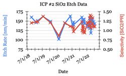
| + | *[https://docs.google.com/spreadsheets/d/1m0l_UK2lDxlgww4f6nfXe4aQedNeDZsLs46jQ5wR4zw/edit#gid=1804752281 SiO2 Etch with CHF3/CF4 - '''Plots'''][[File:ICP2 Process Control Data Example.jpg|alt=example ICP2 process control chart|none|thumb|250x250px|[https://docs.google.com/spreadsheets/d/1m0l_UK2lDxlgww4f6nfXe4aQedNeDZsLs46jQ5wR4zw/edit#gid=1804752281 Click for Process Control Charts]|link=https://docs.google.com/spreadsheets/d/1m0l_UK2lDxlgww4f6nfXe4aQedNeDZsLs46jQ5wR4zw/edit#gid=1804752281]] |
||
| + | |||
==SiO<sub>2</sub> Etching (Panasonic 2)== |
==SiO<sub>2</sub> Etching (Panasonic 2)== |
||
| + | |||
| − | *[[media:Panasonic2-SiOx-Recipe.pdf|SiO<sub>2</sub> Vertical Etch Recipe]] |
||
| + | ===Recipes=== |
||
| + | |||
| + | *[//wiki.nanotech.ucsb.edu/wiki/images/d/d5/Panasonic2-SiOx-Recipe.pdf SiO<sub>2</sub> Vertical Etch Recipe - CHF<sub>3</sub> "SiOVert"] |
||
| + | **Direct copy of "SiOVert" from ICP#1, [[ICP_Etching_Recipes#SiO2_Etching_.28Panasonic_1.29|see parameters there]]. |
||
| + | *[//wiki.nanotech.ucsb.edu/wiki/images/9/9e/33-Etching_SiO2_with_Vertical_Side-wall.pdf SiO<sub>2</sub> Vertical Etch Recipe#2 - CF<sub>4</sub>/CHF<sub>3</sub>] |
||
| + | *[//wiki.nanotech.ucsb.edu/wiki/images/1/1e/Panasonic2-ICP-Plasma-Etch-SiO2-nanoscale-rev1.pdf SiO<sub>2</sub> Nanoscale Etch Recipe - CHF<sub>3</sub>/O<sub>2</sub>] |
||
| + | |||
| + | ===Recipe Variations=== |
||
| + | ''Use these to determine how etch parameters affect the process.'' |
||
| + | |||
| + | *[https://wiki.nanotech.ucsb.edu/wiki/images/1/1e/05-SiO2_Nano-structure_Etch.pdf Angled SiO2 sidewall recipes] |
||
| + | |||
| + | ==SiN<sub>x</sub> Etching (Panasonic 2)== |
||
| + | |||
| + | *[//wiki.nanotech.ucsb.edu/wiki/images/0/06/Panasonic2-ICP-Plasma-Etch-SiN-nanoscale-rev1.pdf SiN<sub>x</sub> Nanoscale Etch Recipe - CHF<sub>3</sub>/O<sub>2</sub>] |
||
| + | |||
| + | ==Al Etch (Panasonic 2)== |
||
| + | |||
| + | *[https://wiki.nanotech.ucsb.edu/wiki/images/3/3b/Panasonic-1-Al-Etch-RevA.pdf Al Etch Recipes - use panasonic 1 parameters, etch rate 50% higher] |
||
| + | |||
| + | ==Al2O3 Etching (Panasonic 2)== |
||
| + | [//wiki.nanotech.ucsb.edu/wiki/images/d/d2/Brian_Markman_-_Al2O3_ICP2_Etch_Rates_2018.pdf ALD Al2O3 Etch Rates in BCl3 Chemistry] (click for plots of etch rate) |
||
| + | |||
| + | ''Contributed by Brian Markman, 2018'' |
||
| + | |||
| + | *BCl3 = 30sccm |
||
| + | *Pressure = 0.50 Pa |
||
| + | *ICP Source RF = 500 |
||
| + | *Bias RF = 50W or 250W (250W can burn PR) |
||
| + | *Cooling He Flow/Pressure = 15.0 sccm / 400 Pa |
||
| + | *Etch Rate 50W: 39.6nm/min (0.66nm/sec) |
||
| + | *Etch Rate 250W: 60.0nm/min (1.0 nm/sec) |
||
| + | |||
| + | ==GaAs Etch (Panasonic 2)== |
||
| + | |||
| + | *[//wiki.nanotech.ucsb.edu/wiki/images/f/ff/16-GaAs_etch-ICP-2.pdf GaAs Etch Recipes - Panasonic 2 - Cl<sub>2</sub>N<sub>2</sub>] |
||
| + | |||
| + | ==Photoresist and ARC etching (Panasonic 2)== |
||
| + | Basic recipes for etching photoresist and Bottom Anti-Reflection Coating (BARC) underlayers are as follows: |
||
| + | |||
| + | ===ARC Etching: DUV-42P or AR6 (Panasonic 2)=== |
||
| + | |||
| + | *O2 = 40 sccm // 0.5 Pa |
||
| + | *ICP = 75W // RF = 75W |
||
| + | *45 sec for full etching (incl. overetch) of ~60nm [[Stepper Recipes#DUV-42P-6|DUV-42P]] (same as for AR6; 2018-2019, [[Demis D. John|Demis]]/[[Brian Thibeault|BrianT]]) |
||
| + | |||
| + | ===Photoresist Etch/Strip (Panasonic 2)=== |
||
| + | Works very well for photoresist stripping |
||
| + | |||
| + | *O2 = 40 sccm // 1.0 Pa |
||
| + | *ICP = 350W // RF = 100W |
||
| + | *Etch Rate for UV6-0.8 (DUV PR) = 518.5nm / 1min (2019, [[Demis D. John|Demis]]) |
||
| + | *2m30sec to fully remove UV6-0.8 with ~200% overetch (2019, [[Demis D. John|Demis]]) |
||
| + | |||
| + | ==Ru (Ruthenium) Etch (Panasonic 2)== |
||
| + | |||
| + | *[https://wiki.nanotech.ucsb.edu/wiki/images/e/e9/194_Ru_Etch_O2%2CCl2.pdf Ru Etch] - ''[[Bill Mitchell]] 2019-09-19'' |
||
| + | **''This etch is used in the following publication:'' [[Template:Publications#Highly Selective and Vertical Etch of Silicon Dioxide using Ruthenium Films as an Etch Mask|W.J. Mitchell, "Highly Selective and Vertical Etch of Silicon Dioxide using Ruthenium Films as an Etch Mask" (JVST-A, 2021)]] |
||
=[[ICP-Etch (Unaxis VLR)]]= |
=[[ICP-Etch (Unaxis VLR)]]= |
||
| − | ==InP Etch (Unaxis VLR)== |
||
| − | ===InP Etch === |
||
| − | *[[media:UNAXIS-VLR-InP-Etch-200C-Recipe.pdf|InP Etch Recipe (200C)]] |
||
| − | ===InP Etch (H<sub>2</sub> Ar)=== |
||
| − | *[[media:UNAXIS-VLR-InP-Etch-Ar-200C-Recipe.pdf|InP Etch Recipe (H<sub>2</sub> Ar 200C)]] |
||
| + | ==Process Control Data (Unaxis VLR)== |
||
| − | =[[Si-Etch (XeF2 Etch (Xetch))]]= |
||
| + | |||
| − | *[[media:06-XeF2-etch-recipe.pdf|Si Etch Recipe]] |
||
| + | *[[Unaxis VLR Etch - Process Control Data|InP Etch - Process Control Data]] |
||
| + | |||
| + | ==GaAs-AlGaAs Etch (Unaxis VLR)== |
||
| + | |||
| + | *[//wiki.nanotech.ucsb.edu/wiki/images/4/4e/15-GaAs_etch-Unaxis_ICP_etcher.pdf GaAs Etch Recipe (Cl<sub>2</sub>N<sub>2</sub> 30C)] |
||
| + | *[//wiki.nanotech.ucsb.edu/wiki/images/1/1f/14-AlAs-GR-cal_etch-Unaxis_ICP_etcher.pdf AlGaAs Etch Recipe (Cl<sub>2</sub>N<sub>2</sub> 30C)] |
||
| + | |||
| + | ==InP-InGaAs-InAlAs Etch (Unaxis VLR)== |
||
| + | |||
| + | *[//wiki.nanotech.ucsb.edu/wiki/images/9/90/18-InP-based_etching-Cl2N2Ar.pdf InP-based Material Etch Profile (Cl<sub>2</sub>N<sub>2</sub>Ar200C)] |
||
| + | *[//wiki.nanotech.ucsb.edu/wiki/images/a/ad/17-InP%26InGaAs_etch-Cl2H2Ar-Unaxis-VLR.pdf InP-InGaAs Etch Profile (Cl<sub>2</sub>H<sub>2</sub>Ar 200C)] |
||
| + | *[//wiki.nanotech.ucsb.edu/wiki/images/6/6e/SiO2-Mask_Etch_Recipe_for_Unaxis_Cl2_Etch.pdf Recipe of Etching SiO<sub>2</sub> Mask for Cl<sub>2</sub> Etch (ICP#2)] |
||
| + | *[[InP Etch Test Result in Details|InP Etch Historical Data (Cl<sub>2</sub>H<sub>2</sub>Ar 200C)]] |
||
| + | *[[InP Etch Rate and Selectivity (InP/SiO2)|InP Etch Test]] |
||
| + | *[//wiki.nanotech.ucsb.edu/wiki/images/a/ac/Lower-Etch-Rate_InP_Etch_using_Unaxis_PM1_tool_at_200_C.pdf Lower etch-rate InP Etch (Cl<sub>2</sub>N<sub>2</sub> 200C)] |
||
| + | |||
| + | ==GaN Etch (Unaxis VLR)== |
||
| + | |||
| + | *[//wiki.nanotech.ucsb.edu/wiki/images/d/df/09-Plasma_Etching_of_GaN-UnaxisPM1.pdf GaN Etch Recipe (Cl<sub>2</sub>BCl<sub>3</sub>N<sub>2</sub>Ar 85C)] |
||
| + | |||
| + | ==GaSb Etch (Unaxis VLR)== |
||
| + | ''Available - ask staff'' |
||
| + | |||
| + | ==Cleaning Recipes (Unaxis VLR)== |
||
| + | ''To Be Added: Required cleaning time & recipes'' |
||
| + | |||
| + | =[[Oxford ICP Etcher (PlasmaPro 100 Cobra)]]= |
||
| + | |||
| + | ==Process Control Data (Oxford ICP Etcher)== |
||
| + | |||
| + | ===[https://docs.google.com/spreadsheets/d/1cEUB7K5BAg9N4vp3rPZw7g0orFkxeQmRkX34Fb4eZco/edit#gid=1804752281 Process Control Data for "Std InP Ridge Etch" Cl<sub>2</sub>/CH<sub>4</sub>/H<sub>2</sub>/60°C]=== |
||
| + | ''Calibration / Process testing data taken using the "InP Ridge Etch" process: Cl2/CH4/H2 @ 60°C, 1cm piece with ~50% SiO2 hardmask.'' |
||
| + | |||
| + | *[https://docs.google.com/spreadsheets/d/1cEUB7K5BAg9N4vp3rPZw7g0orFkxeQmRkX34Fb4eZco/edit?usp=sharing "Std InP Ridge Etch" Cl<sub>2</sub>/CH<sub>4</sub>/H<sub>2</sub>/60°C - '''Etch Data Tables'''] |
||
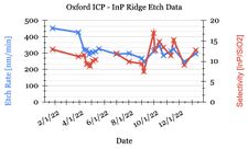
| + | *[https://docs.google.com/spreadsheets/d/1cEUB7K5BAg9N4vp3rPZw7g0orFkxeQmRkX34Fb4eZco/edit#gid=1804752281 "Std InP Ridge Etch" Cl<sub>2</sub>/CH<sub>4</sub>/H<sub>2</sub>/60°C - '''Plots'''][[File:Oxford-ICP-Etch Process Control Data Example.jpg|alt=example SPC chart for Oxford ICP Etcher|none|thumb|225x225px|[https://docs.google.com/spreadsheets/d/1cEUB7K5BAg9N4vp3rPZw7g0orFkxeQmRkX34Fb4eZco/edit#gid=1804752281 Click for Process Control Charts]|link=https://docs.google.com/spreadsheets/d/1cEUB7K5BAg9N4vp3rPZw7g0orFkxeQmRkX34Fb4eZco/edit#gid=1804752281]] |
||
| + | |||
| + | ==InP Ridge Etch (Oxford ICP Etcher)== |
||
| + | ===Low-Temp (60°C) Process=== |
||
| + | |||
| + | *[[Media:Oxford Etcher - InP Ridge Etch using Oxford PlasmaPro 100 Cobra - 2021-09-08.pdf|Low-Temp InP Ridge Etch Characterization]] - ''Ning Cao, 2021-09-08'' |
||
| + | **InP etches were characterized with '''no''' mounting adhesive used, 1/4-wafer of 50mm wafer placed on blank Silicon carriers (rough side up). |
||
| + | **Recipe: Cl2/CH4/H2 - 60°C |
||
| + | **NOTE: Rates in these 2021-09 characterizations are lower than current due to a software timing bug, fixed in 2022-01 |
||
| + | *See [[Oxford ICP Etcher (PlasmaPro 100 Cobra)#Documentation|Operating Procedure]] for full traveler and post-cleaning. |
||
| + | |||
| + | ====[[Oxford Etcher - Sample Size Effect on Etch Rate|Sample Size effect on Etch Rate]]==== |
||
| + | ''See the above table for data showing effect on sample size/exposed etched area.'' |
||
| + | |||
| + | ==InP Grating Etch (Oxford ICP Etcher)== |
||
| + | |||
| + | *[[Media:Oxford Etcher - InP Grating Etch at 20 C - Oxford Cobra 300 2021-08-26.pdf|InP/InGaAsP Grating Etch Characterization]] - ''Ning Cao, 2021-08-26'' |
||
| + | **InP/InGaAsP etches were characterized with '''no''' mounting adhesive used, 1/4-wafer of 50mm wafer placed on Silicon carriers (rough side up). |
||
| + | **Recipe: Cl2/CH4/H2/Ar - 20°C |
||
| + | **NOTE: Rates in these 2021-09 characterizations are lower than current due to a software timing bug, fixed in 2022-01 |
||
| + | *See [[Oxford ICP Etcher (PlasmaPro 100 Cobra)#Documentation|Operating Procedure]] for full traveler and post-cleaning. |
||
| + | |||
| + | ==GaAs Etch (Oxford ICP Etcher)== |
||
| + | This recipe also provides a starting point for '''GaSb'''-based etches. |
||
| + | |||
| + | *GaAs-based materials - etch recipe available on tool - ''provided by Oxford, not yet qualified internally'' |
||
| + | *See [[Oxford ICP Etcher (PlasmaPro 100 Cobra)#Documentation|Operating Procedure]] for full traveler and post-cleaning. |
||
| + | |||
| + | ==GaN Etch (Oxford ICP Etcher)== |
||
| + | |||
| + | *GaN-based materials - etch recipe available on tool - ''provided by Oxford, not yet qualified internally'' |
||
| + | *See [[Oxford ICP Etcher (PlasmaPro 100 Cobra)#Documentation|Operating Procedure]] for full traveler and post-cleaning. |
||
| + | |||
| + | ==GaN Atomic Layer Etching (Oxford ICP Etcher)== |
||
| + | ''GaN-ALE Recipe written and tested by users - contact [[Tony Bosch|supervisor]] for use.'' |
||
| + | |||
| + | ==Cleaning Recipes (Oxford ICP Etcher)== |
||
| + | '''''To Be Added: Required cleaning time & recipes''''' |
||
| + | |||
| + | =[[Si Deep RIE (PlasmaTherm/Bosch Etch)|Si Deep RIE (PlasmaTherm/Bosch Etch) - DECOMISSIONED]]= |
||
| + | '''This tool does not exist in this configuration any more, so these recipes are for Reference purposes Only!!!''' |
||
| + | The machine was upgraded to be the new Plasma-Therm Fluorine ICP Etcher - the chamber configuration is now different, making these recipes invalid. |
||
| + | For Deep Silicon Etching, the [[ICP Etching Recipes#High Rate Bosch Etch .28DSEIII.29|Plasma-Therm DSE-iii]] is often used. Some single-step Silicon etching is still performed on the [[ICP Etching Recipes#Si Etching .28Fluorine ICP Etcher.29|SLR Fluorine ICP]], due to the slower etch rate. |
||
| + | |||
| + | ==Bosch and Release Etch (Si Deep RIE)== |
||
| + | |||
| + | *[//wiki.nanotech.ucsb.edu/wiki/images/0/02/10-Si_Etch_Bosch_Release_DRIE.pdf Bosch and Release Processes] |
||
| + | **Ideal for deep (>>1µm), vertical etching of Silicon. Through-wafer etches are possible (requires carrier wafer). |
||
| + | **Etch rate depends on area of exposed silicon being etched. |
||
| + | **Al<sub>2</sub>O<sub>3</sub> mask (ALD or Sputter) has >9000:1 selectivity |
||
| + | **SiO<sub>2</sub> (PECVD) mask has ~100:1 selectivity |
||
| + | **Thermal SiO<sub>2</sub> has ~300:1 selectivity. |
||
| + | |||
| + | ==Single-step Si Etching (not Bosch Process!) (Si Deep RIE)== |
||
| + | |||
| + | *[//wiki.nanotech.ucsb.edu/wiki/images/d/d2/10-Si_Etch_using_DRIE_%28single-step%29.pdf Single-step Si Vertical Etch Recipe - SF<sub>6</sub>-C<sub>4</sub>F<sub>8</sub>-Ar] |
||
Latest revision as of 17:09, 9 April 2024
Back to Dry Etching Recipes.
DSEIII_(PlasmaTherm/Deep_Silicon_Etcher)
Process Control Data (DSEiii)
Edge-Bead Removal (DSEiii)
Make sure to remove photoresist from edges of wafer, or PR may stick to the top-side wafer clamp and destroy your wafer during unload!
- Edge Bead Removal via Photolithography: use a custom metal mask to pattern the photoresist with a flood exposure.
- If you are etching fully through a wafer, remember that removal of edge-bead will cause full etching in the exposed areas. To prevent a wafer from falling into the machine after the etch, you can mount to a carrier wafer using wax.
- Manual PR Edge-Bead Removal - using swabs and EBR100. This is prone to error and easy to accidentally leave a blob of PR on the edge - so be extra careful to ensure NO PR is left on the edges!
High Rate Bosch Etch (DSEIII)
- Bosch Process Recipe and Characterization - Standard recipe on the tool.
- Recipe Name: "Plasma-Therm Standard DSE" (Production - copy to your Personal category)
- Standard Bosch Process for high aspect-ratio, high-selectivity Silicon etching.
- Cycles between polymer deposition "Dep" / Polymer etch "Etch A" / Si etch "Etch B" steps. Step Times gives fine control.
- To reduce roughening/grassing (black silicon), reduce Dep step time by ~20%.
- Patterns with different exposed/etched areas will have different "optimal" parameters.
- Approx Selectivity to Photoresist: ~80 or better.
- Larger open area, lower selectivity and lower etch rate.
- Thick PR's approx ≥10µm tend to burn, avoid thick PR's. They also make edge-bead removal very difficult.
- Selectivity to SiO2 should be higher, not yet measured.
- Selectivity to Al2O3 is extremely high, >9000. See below TSV process for processing notes on this film.
- If you need to pattern all the way to the edge of the wafer, PR won't work because you have to remove the edge-bead of photoresist (see above). Instead use hardmask process (See "Through Silicon Via" etch below).

Through Silicon Via (TSV) etch (DSEiii)
Since the topside clamp requires the removal of photoresist on the outermost ~5-7mm of the wafer, this makes PR incompatible with through-silicon etching (as the outer edges would be etched-through, dropping the inner portion into the chamber). In addition, in practice we have found that thick PR often roughens and burns during long ~30-60min etches, making removal very difficult.
Instead, we recommend the following process with Al2O3 hardmask:
NOTE: We have recently found that the wax-mounting process process can leave wax on the wafer clamp, causing the next user's wafer to get stuck and fail transfer! DO NOT RUN the wax-mounting process without discussing with staff first. (Through-wafer process with no wax is still acceptable.) -- Demis 2024-03-11
| Process for Through-Wafer Silicon Etching | |
|---|---|
| Process to etch through ~550µm Silicon | Demis D. John & Biljana Stamenic 2022-11-11. Please consider our publication policy if you use/modify this process. |
Deposit 150nm Al2O3 on either:
|
May need to do dep. rate check beforehand. |
| Deposit ~3nm SiO2, in situ (same machine as above) | This improves adhesion to photoresist and prevents developer attacking the Al2O3. |
| Lithography - your preferred method. Needs approx. ≥500nm thick PR. | |
| Etch the Al2O3 in Panasonic ICP 1/2 | Use 50W version. Overetch by ~20%, will also etch through the thin SiO2 layer. |
| Strip PR - either in situ, or via NMP 80°C soak followed by PEii Technics ashing. | In situ PR strip appears to give better + faster results. |
| If pieces of the wafer are at risk of falling into the chamber, mount the product wafer to a carrier wafer:
Logitech Wax Mounting Recipe - Bulk Crystal Bond
|
Critical - Ensure no wax is present on either side or edge of wafer prior to DSE etching, or wafer may break in the DSE during robot unload! |
| Use POLOS spinners with ACE/ISO to clean front and back of wafer.
IMPORTANT for wax-mounting, to ensure wax does not stick your wafer to the DSE clamp. Observe carefully for any wax protruding from between wafers - redo spin-clean as needed. |
Also make sure wax thickness is not too thick, of long etches could cause wax to seep out from between the wafers. |
DSEiii etch - reduce Dep step to eliminate grassing:
|
Can use Lasermonitor and/or Camera to observe when etch is fully through. Trenches may get black/rough, but then clear up when fully etched.
Record Helium FLOW during recipe run, for next step (if He leaks). Ok to remove wafer, observe/measure, and re-load for etching. If see black grass and etch rate drops, may need to run an O2 plasma with Technics PEii few min to remove polymer, reduce Dep step time and then continue. |
| If you did not wax-mount your wafer, the recipe will eventually fail for Helium Pressure/Flow our of compliance. This is because the cooling Helium leaks through the wafer when the openings get fully etched through.
Once this happens,
|
|
| Strip Al2O3/SiO2 either with HF, or same Pan1/2 dry etch as above. | |
IF wax-mounted - either
OR
|
|
| If you publish using the above process, please consider our publication policy. This process was developed by Biljana Stamenic and Demis D. John, 2022. | |
Single-Step Low Etch Rate Smooth Sidewall Process (DSEIII)
- Single Step Silicon Etch Recipe and Characterization
- Recipe Name: "Nano Trench Etch" (Production - copy to your Personal category)
- Used instead of Bosch Process, to avoid scalloping on the sidewall.
- Lower selectivity, lower etch rate, smoother sidewalls.
PlasmaTherm/SLR Fluorine Etcher
Recipe Tips
- RF1: Bias Power (with DCV readback)
- RF2: ICP Power
- For trouble igniting ICP plasma, add 15 to 75 W of bias power during ignition step. Typical ignition pressures 5 to 10 mT.
Process Control Data (Fluorine ICP Etcher)
SiO2 Etching with CHF3/CF4 (Fluorine ICP Etcher)
Si Etching (Fluorine ICP Etcher)
- SiVertHF - Si Vertical Etch using C4F8/SF6/CF4 and resist mask
- Etch Rates: Si ≈ 300-350 nm/min; SiO2 ≈ 30-35 nm/min
- 89-90 degree etch angle, ie, vertical.
- High selectivity to Al2O3 masks.
Process Notes/Observations
- Due to high selectivity against SiO2, it may be necessary to run a ~10sec 50W SiO2 etch (below) to remove native oxide on Si. This can be performed in situ before the Si etch.
- We have observed that full-wafers with small open area in photoresist masks might require a recalibration of the C4F8/SF6 ratio in order to prevent very low etch rates.
SiO2 Etching (Fluorine ICP Etcher)
- SiO2 Etching using Ruthenium Hardmask - Full Process Traveler
- Ning Cao & Bill Mitchell, 2019-06
- High-selectivity and deep etching using sputtered Ru hardmask and I-Line litho.
- Etch also works well with PR masking
- Chemistry: CHF3/CF4
- Variations in SiO2 etch Bias Power: 50 / 200 / 400W bias.
- Ru etch selectivity to PR: 0.18 (less than 1): 150nm Ru / 800nm PR
- 50W Bias: (recommended)
- Selectivity to photoresist: 1.10–1.20
- SiO2 selectivity to Ru: 36
- SiO2 etch rate: 263nm/min
- 200W Bias:
- SiO2 selectivity to Ru: 38
- SiO2 etch rate: 471nm/min
- This etch is detailed in the following article: W.J. Mitchell et al., JVST-A, May 2021
Si3N4 Etching (Fluorine ICP Etcher)
Developed by Bill Mitchell. Please see publication policy.
- ICP = 950/75W
- Pressure = 5mT
- Low Polymer Dep: CF4 = 60sccm
- Etch Rate = 420nm/min (PECVD Si3N4)
- Higher verticality: CF4 = 35 / CHF3 = 25 sccm
- Etch Rate = 380nm/min (PECVD Si3N4)
Photoresist & ARC (Fluorine ICP Etcher)
Chain multiple Recipes in a Flow, to allow you to to do in situ BARC etching, and follow up with in situ Photoresist Strip.
PR/BARC Etch (Fluorine ICP Etcher)
- Etching DUV42P-6 Bottom Anti-Reflection Coating
- ~60nm thick (2500krpm)
- O2=20sccm / 10mT / RF1(bias)=100W / RF2(icp)=0W
- 1min
Photoresist Strip/Polymer Removal (Fluorine ICP Etcher)
- O2=100sccm / 5mT / RF1(bias)=10W / RF2(icp)=825W
- 75W Bias can be helpful for difficult to remove polymers, eg. 2min
- Use laser monitor to check for complete removal, overetch to remove Fluorocarbon polymers.
Cleaning Procedures (Fluorine ICP Etcher)
To Be Added
ICP Etch 1 (Panasonic E646V)
Process Control Data (Panasonic 1)
SiO2 Etch with CHF3/CF4 - Process Control Data (Panasonic 1)
SiO2 Etching (Panasonic 1)
Recipes
- SiO2 Vertical Etch Recipe Parameters - CHF3 "SiOVert"
- Etch rate ≈ 2300Å/min (users must calibrate)
- Selectivity (SiO2:Photoresist) ≈ greater than 1:1 (users must calibrate)
Recipe Variations
Use these to determine how each etch parameter affects the process.
- SiO2 CHF3 Etch Variations - CHF3 with varying Bias and Pressure, Slanted SiO2 etching
SiNx Etching (Panasonic 1)
Al Etch (Panasonic 1)
Cr Etch (Panasonic 1)
Ta Etch (Panasonic 1)
- Ta Etch Recipe - Cl2/BCl3
Ti Etch (Panasonic 1)
W-TiW Etch (Panasonic 1)
GaAs-AlGaAs Etch (Panasonic 1)
- GaAs-Nanoscale Etch Recipe - PR mask - Cl2-BCl3-Ar
- AlGaAs Etch Recipes - Cl2N2
- GaAs DRIE via Etch Recipes - Cl2-BCl3-Ar PR passivation
GaN Etch (Panasonic 1)
Photoresist and ARC Etching (Panasonic 1)
Please see the recipes for Panasonic ICP#2 - the same recipes apply.
Etching of DUV42P at standard spin/bake parameters also completes in 45 seconds.
SiC Etch (Panasonic 1)
Sapphire Etch (Panasonic 1)
Cleaning Recipes
To Be Added
Old Deleted Recipes
Since there are a limited number of recipe slots on the tool, we occasionally have to delete old, unused recipes.
If you need to free up a recipe slot, please contact the tool's Supervisor and they'll help you find an old recipe to replace. We take photographs of old recipes, and save them in case a group needs to revive the recipe. Contact us if your old recipe went missing.
ICP Etch 2 (Panasonic E626I)
Recipes starting points for materials without processes listed can be obtained from Panasonic1 recipe files. The chambers are slightly different, but essentially the same, requiring only small program changes to obtain similar results.
Process Control Data (Panasonic 2)
SiO2 Etch with CHF3/CF4 - Process Control Data (Panasonic 2)
SiO2 Etching (Panasonic 2)
Recipes
- SiO2 Vertical Etch Recipe - CHF3 "SiOVert"
- Direct copy of "SiOVert" from ICP#1, see parameters there.
- SiO2 Vertical Etch Recipe#2 - CF4/CHF3
- SiO2 Nanoscale Etch Recipe - CHF3/O2
Recipe Variations
Use these to determine how etch parameters affect the process.
SiNx Etching (Panasonic 2)
Al Etch (Panasonic 2)
Al2O3 Etching (Panasonic 2)
ALD Al2O3 Etch Rates in BCl3 Chemistry (click for plots of etch rate)
Contributed by Brian Markman, 2018
- BCl3 = 30sccm
- Pressure = 0.50 Pa
- ICP Source RF = 500
- Bias RF = 50W or 250W (250W can burn PR)
- Cooling He Flow/Pressure = 15.0 sccm / 400 Pa
- Etch Rate 50W: 39.6nm/min (0.66nm/sec)
- Etch Rate 250W: 60.0nm/min (1.0 nm/sec)
GaAs Etch (Panasonic 2)
Photoresist and ARC etching (Panasonic 2)
Basic recipes for etching photoresist and Bottom Anti-Reflection Coating (BARC) underlayers are as follows:
ARC Etching: DUV-42P or AR6 (Panasonic 2)
- O2 = 40 sccm // 0.5 Pa
- ICP = 75W // RF = 75W
- 45 sec for full etching (incl. overetch) of ~60nm DUV-42P (same as for AR6; 2018-2019, Demis/BrianT)
Photoresist Etch/Strip (Panasonic 2)
Works very well for photoresist stripping
- O2 = 40 sccm // 1.0 Pa
- ICP = 350W // RF = 100W
- Etch Rate for UV6-0.8 (DUV PR) = 518.5nm / 1min (2019, Demis)
- 2m30sec to fully remove UV6-0.8 with ~200% overetch (2019, Demis)
Ru (Ruthenium) Etch (Panasonic 2)
- Ru Etch - Bill Mitchell 2019-09-19
- This etch is used in the following publication: W.J. Mitchell, "Highly Selective and Vertical Etch of Silicon Dioxide using Ruthenium Films as an Etch Mask" (JVST-A, 2021)
ICP-Etch (Unaxis VLR)
Process Control Data (Unaxis VLR)
GaAs-AlGaAs Etch (Unaxis VLR)
InP-InGaAs-InAlAs Etch (Unaxis VLR)
- InP-based Material Etch Profile (Cl2N2Ar200C)
- InP-InGaAs Etch Profile (Cl2H2Ar 200C)
- Recipe of Etching SiO2 Mask for Cl2 Etch (ICP#2)
- InP Etch Historical Data (Cl2H2Ar 200C)
- InP Etch Test
- Lower etch-rate InP Etch (Cl2N2 200C)
GaN Etch (Unaxis VLR)
GaSb Etch (Unaxis VLR)
Available - ask staff
Cleaning Recipes (Unaxis VLR)
To Be Added: Required cleaning time & recipes
Oxford ICP Etcher (PlasmaPro 100 Cobra)
Process Control Data (Oxford ICP Etcher)
Process Control Data for "Std InP Ridge Etch" Cl2/CH4/H2/60°C
Calibration / Process testing data taken using the "InP Ridge Etch" process: Cl2/CH4/H2 @ 60°C, 1cm piece with ~50% SiO2 hardmask.
- "Std InP Ridge Etch" Cl2/CH4/H2/60°C - Etch Data Tables
- "Std InP Ridge Etch" Cl2/CH4/H2/60°C - Plots
InP Ridge Etch (Oxford ICP Etcher)
Low-Temp (60°C) Process
- Low-Temp InP Ridge Etch Characterization - Ning Cao, 2021-09-08
- InP etches were characterized with no mounting adhesive used, 1/4-wafer of 50mm wafer placed on blank Silicon carriers (rough side up).
- Recipe: Cl2/CH4/H2 - 60°C
- NOTE: Rates in these 2021-09 characterizations are lower than current due to a software timing bug, fixed in 2022-01
- See Operating Procedure for full traveler and post-cleaning.
Sample Size effect on Etch Rate
See the above table for data showing effect on sample size/exposed etched area.
InP Grating Etch (Oxford ICP Etcher)
- InP/InGaAsP Grating Etch Characterization - Ning Cao, 2021-08-26
- InP/InGaAsP etches were characterized with no mounting adhesive used, 1/4-wafer of 50mm wafer placed on Silicon carriers (rough side up).
- Recipe: Cl2/CH4/H2/Ar - 20°C
- NOTE: Rates in these 2021-09 characterizations are lower than current due to a software timing bug, fixed in 2022-01
- See Operating Procedure for full traveler and post-cleaning.
GaAs Etch (Oxford ICP Etcher)
This recipe also provides a starting point for GaSb-based etches.
- GaAs-based materials - etch recipe available on tool - provided by Oxford, not yet qualified internally
- See Operating Procedure for full traveler and post-cleaning.
GaN Etch (Oxford ICP Etcher)
- GaN-based materials - etch recipe available on tool - provided by Oxford, not yet qualified internally
- See Operating Procedure for full traveler and post-cleaning.
GaN Atomic Layer Etching (Oxford ICP Etcher)
GaN-ALE Recipe written and tested by users - contact supervisor for use.
Cleaning Recipes (Oxford ICP Etcher)
To Be Added: Required cleaning time & recipes
Si Deep RIE (PlasmaTherm/Bosch Etch) - DECOMISSIONED
This tool does not exist in this configuration any more, so these recipes are for Reference purposes Only!!!
The machine was upgraded to be the new Plasma-Therm Fluorine ICP Etcher - the chamber configuration is now different, making these recipes invalid.
For Deep Silicon Etching, the Plasma-Therm DSE-iii is often used.  Some single-step Silicon etching is still performed on the SLR Fluorine ICP, due to the slower etch rate.
Bosch and Release Etch (Si Deep RIE)
- Bosch and Release Processes
- Ideal for deep (>>1µm), vertical etching of Silicon. Through-wafer etches are possible (requires carrier wafer).
- Etch rate depends on area of exposed silicon being etched.
- Al2O3 mask (ALD or Sputter) has >9000:1 selectivity
- SiO2 (PECVD) mask has ~100:1 selectivity
- Thermal SiO2 has ~300:1 selectivity.