Difference between revisions of "ICP Etch 1 (Panasonic E646V)"
Reynolds t (talk | contribs) (Undo revision 153650 by Reynolds t (talk)) |
Reynolds t (talk | contribs) |
||
| Line 11: | Line 11: | ||
= About = |
= About = |
||
| ⚫ | This is a three-chamber tool for etching of a variety of materials. Chamber one is configured as an ICP etching tool with 1000 W ICP power, 500 W RF substrate power, and RT - 80°C operation with back-side He cooling and an electrostatic chuck to maintain controlled surface temperatures during etching. This chamber has Cl<sub>2</sub>, BCl<sub>3</sub>, CF<sub>4</sub>, CHF<sub>3</sub>, SF<sub>6</sub>, Ar, N<sub>2</sub>, and O<sub>2 </sub>for gas sources and can be used to etch a variety of materials from SiO<sub>2</sub> to metals to compound semiconductors. The chamber evacuated with a 2000 lpm Osaka Vacuum magnetically levitated turbo pump, allowing for fast pump down. Chamber two is a 2000 W ICP chamber configures for plasma etching of photoresist and other materials such as BCB. The substrate is not biased and the chamber has CF<sub>4</sub> and O<sub>2</sub> for the gases. Chamber three is a DI rinsing chamber for rinsing off any etch byproducts before removing the sample from the system. The system accepts 6” wafers or pieces mounted to the wafers. In Automatic mode, multiple wafers can be run through automatically with the cassette-based system.of low-stress Nitride films. |
||
| − | |||
| ⚫ | This is a |
||
= Detailed Specifications = |
= Detailed Specifications = |
||
| − | * |
+ | *1000 W ICP source, 500 W RF Sample Bias Source in etching chamber |
| − | *RT - 80°C sample temperature for etching |
+ | *RT - 80°C sample temperature for etching |
| + | *Optimal Emission Monitoring |
||
| − | *Etch pressure from 0.1 Pa to 5 Pa (0.75 mT - 37.5 mT) |
+ | *Etch pressure from 0.1 Pa to 5 Pa (0.75 mT - 37.5 mT) |
| − | *Cl<sub>2</sub>, BCl<sub>3</sub>, CF<sub>4</sub>, CHF<sub>3</sub>, SF<sub>6</sub>, Ar, N<sub>2</sub> |
+ | *Cl<sub>2</sub>, BCl<sub>3</sub>, CF<sub>4</sub>, CHF<sub>3</sub>, SF<sub>6</sub>, Ar, N<sub>2</sub>, and O<sub>2</sub> in etch chamber |
| + | *2000 W ICP ashing chamber |
||
| + | *RT - 250°C sample temperature for ashing |
||
| + | *Ashing pressures 50 mT - 500 mT |
||
| + | *O<sub>2</sub>, N<sub>2</sub>, CF<sub>4</sub>, H<sub>2</sub>O Vapor for ashing chamber |
||
| + | *Multiple 6” diameter wafer capable system |
||
*Pieces possible by mounting to 6” wafer |
*Pieces possible by mounting to 6” wafer |
||
| + | |||
| − | *Load-Locked |
||
| + | |||
| − | *Up to 20 steps per recipe |
||
| − | *Laser monitor with 679.60nm wavelength |
||
=Documentation= |
=Documentation= |
||
Revision as of 16:08, 13 June 2015
| |||||||||||||||||||||
About
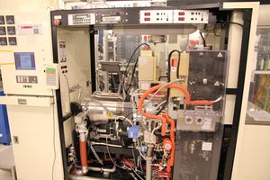
This is a three-chamber tool for etching of a variety of materials. Chamber one is configured as an ICP etching tool with 1000 W ICP power, 500 W RF substrate power, and RT - 80°C operation with back-side He cooling and an electrostatic chuck to maintain controlled surface temperatures during etching. This chamber has Cl2, BCl3, CF4, CHF3, SF6, Ar, N2, and O2 for gas sources and can be used to etch a variety of materials from SiO2 to metals to compound semiconductors. The chamber evacuated with a 2000 lpm Osaka Vacuum magnetically levitated turbo pump, allowing for fast pump down. Chamber two is a 2000 W ICP chamber configures for plasma etching of photoresist and other materials such as BCB. The substrate is not biased and the chamber has CF4 and O2 for the gases. Chamber three is a DI rinsing chamber for rinsing off any etch byproducts before removing the sample from the system. The system accepts 6” wafers or pieces mounted to the wafers. In Automatic mode, multiple wafers can be run through automatically with the cassette-based system.of low-stress Nitride films.
Detailed Specifications
- 1000 W ICP source, 500 W RF Sample Bias Source in etching chamber
- RT - 80°C sample temperature for etching
- Optimal Emission Monitoring
- Etch pressure from 0.1 Pa to 5 Pa (0.75 mT - 37.5 mT)
- Cl2, BCl3, CF4, CHF3, SF6, Ar, N2, and O2 in etch chamber
- 2000 W ICP ashing chamber
- RT - 250°C sample temperature for ashing
- Ashing pressures 50 mT - 500 mT
- O2, N2, CF4, H2O Vapor for ashing chamber
- Multiple 6” diameter wafer capable system
- Pieces possible by mounting to 6” wafer
