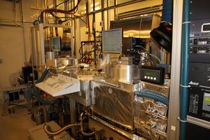
ICP-PECVD (Unaxis VLR)
| |||||||||||||||||||||
About
This system is configured as an ICP PECVD deposition tool with 1000 W ICP power, 600 W RF substrate power, and 100°C-350°C operation. This chamber has 100% SiD4, N2, O2, and Ar for gas sources. The high density PECVD produces a more dense, higher quality SiO2 and Si3N4, as compared with conventional PECVD. With the high density plasma, deposition of high quality films can be deposited as low as 100°C for processes requiring lower temperatures. Stress compensation for silicon nitride is characterized.
Cluster Configuration
A Deposition and Etch chamber are both attached to the same loadlock, allowing etching and deposition without breaking vacuum. Each chamber can be scheduled separately on SignupMonkey.
- PM3: ICP-PECVD Deposition (this page)
- PM1: ICP Etch (Unaxis VLR)
Detailed Specifications
- 1000W ICP source, 600W RF Sample Bias Power Supply
- 100 - 350°C sample temperature
- 100% SiD4, Ar, N2, O2
- Multiple 4” diameter wafer capable system
- Pieces possible by mounting or placing on 4 ” wafer
Documentation
- Operating Instructions
- Unaxis wafer coating procedure - process flow for achieving high-quality coatings.
- For particle counting procedure, see the Surfscan Scanning Procedure
Recipes
You can find recipes for this tool on the Wiki > Recipes > PECVD Recipes page
