IBD: Calibrating Optical Thickness
Basic method for calibrating optical thickness, for DBR/multi-layer optical coatings (2 films only). Commonly used for SiO2/TaO DBR mirrors.
- Get dep rate & refractive index (RIX) of individual SiO and TaO films, using single-deps and J.A. Woolam Ellipsometer or equivalent tool. Approx. rate from previous user is also acceptable.
- Get RIX at the target wavelength, using "Derived Params" on JAW or Cauchy equation A/B/C params. For example, if targeting a DBR centered at 1550nm (target λ=1550nm), you will want to know the RIX at 1550nm specifically.
- Calculate approximate dep. time to achieve a 1/4-wave thickness at the target wavelength, for each film (SiO and TaO).
- For example, if SiO2 measured at 5.2nm/min and RIX is n1550 = 1.494, then SiO 1/4λ thickness: d1/4λ = 1550nm / 4 / 1.494 = 259.4nm SiO 1/4λ time: t1/4λ = 259.4nm ÷ 5.2nm/min = 49.88min = 2993.077 sec (and do the same for TaO)
- Deposit a fabry-perot 1/2-λ of one film (SiO or TaO) cavity onto a Silicon piece, using the above 1/4-λ times (aka. SiO/4 or TaO/4), to calibrate that film's optical-thickness.
- eg. for SiO Fabry-Perot cavity (aka. SiO-FP) SiO/4 + TaO/4 + SiO/4 + TaO/4 + SiO/4 + TaO/4 + (SiO/4 + SiO/4) + TaO/4 + SiO/4 + TaO/4 + SiO/4 + TaO/4 Here we used only 3 periods of DBR on either side of the 1/2-λ cavity, to speed up the deposition.
- Measure the reflectivity on Filmetrics F10-RT.
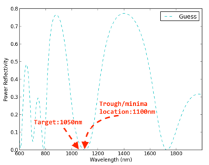
- Locate the wavelength of the minimum (dip) in the optical spectrum. Spectrum will typically be very broad, due to omitting many of the DBR layers for speed.
- For example, the trough might show a minimum at 1600nm. Here is an example of a Fabry-Perot cavity that was targeting a 1050nm, and measured a 1100nm trough:In this case, one would apply a correction to the SiO/4 time by multiplying by 1050÷1000.
- Correct the film's optical thickness as so: t1/4λ * λtarget / λmeasured = corrected t1/4λ 2993.077 sec * 1550nm / 1600nm = 2899.543 sec for SiO/4 layers
- Use this corrected time for all SiO/4 layers.
- Do the same Fabry-Perot correction for the other film, in this case TaO-FP, and apply the new TaO/4 time to the recipe.
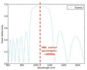
- Perform a test-DBR deposition onto Silicon, eg. 9 periods (less than full, which may be 15 periods), to confirm that center wavelength is in the right spot. An example DBR test-dep targeting 1050nm looks like this:
Sources of error: thick, stressy films exhibit the stress-optic effect, in which compressed films (closer to the substrate) will often show a reduction in RIX. In going from a 9-period DBR to a 18-period DBR, you might see a ~10-20nm blue-shift. Some users for who such a shift is outside the device tolerance will do a full DBR dep, then apply a % reduction to all dep time to further dial in the DBR reflectivity band.
The same method can be used to calibrate optical-thickness for arbitrary binary multi-layer optical filters.
Note, you can verify/better understand the above method using any electromagnetic thin-film simulator. For example, EMpy has a simple transfer-matrix example for doing this, along with RIX models contributed by Demis. Demis created the above simulations using EMpy.
Developed by Demis D. John, Bob Farrell, Dustin Kleckner. This is the same method used by UCSB VCSEL groups years earlier, for calibrating VCSEL MOCVD/MBE growths.

