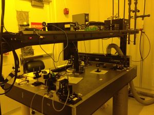
Holographic Lith/PL Setup (Custom)
|
About
The interference lithography system (aka. Holography) at UCSB uses a 15mW, single-mode, 325 nm HeCd laser that is filtered and expanded by pinhole filters to produce the large area exposure beam. The system uses a simple mirror configuration with a fixed 90 degree angle between the mirror and sample. The entire mirror/sample assembly is rotated in 0.1 degree increments to change the grating pitch from ~ 200 nm to ~ 280 nm (35 to 55 degrees) over an ~ 2 cm x 2 cm exposure area.
THMR-3600HP resist spin-coated to ~ 80 nm thickness is used for grating exposure. 2-D gratings can be formed by rotating the sample and doing multiple exposures. Total exposure times are controlled by a manual shutter and are generally several minutes in length.
A photoluminescence measurement setup is co-located on the optical table. Please see the page for the PL system for more info:
Detailed Specifications
- 15 mW single TEM mode HeCd laser
- ~ 2 cm x 2 cm uniform exposure area
- ~ several minute exposure times
- Grating period adjustable from ~200 to ~280 nm with a single stage
