Difference between revisions of "Field Emission SEM 2 (JEOL IT800SHL)"
Jump to navigation
Jump to search
(→Mechanical: added limited 4-inch wf movemnt) |
m |
||
| (6 intermediate revisions by 3 users not shown) | |||
| Line 1: | Line 1: | ||
| − | {{ |
+ | {{tool2|{{PAGENAME}} |
| − | |picture= |
+ | |picture=SEM1_JEOL_IT800HSL.jpg |
|type = Inspection, Test and Characterization |
|type = Inspection, Test and Characterization |
||
|super= Aidan Hopkins |
|super= Aidan Hopkins |
||
| + | |super2= Bill Mitchell |
||
| − | |phone= (805)893-4974 |
||
|location=Bay 1 |
|location=Bay 1 |
||
| − | |email=hopkins@ece.ucsb.edu |
||
|description = JEOL 7600F FESEM |
|description = JEOL 7600F FESEM |
||
|manufacturer = [http://www.jeolusa.com/PRODUCTS/ElectronOptics/ScanningElectronMicroscopesSEM/FESEM/JSM7600F/tabid/544/Default.aspx JEOL USA Inc] |
|manufacturer = [http://www.jeolusa.com/PRODUCTS/ElectronOptics/ScanningElectronMicroscopesSEM/FESEM/JSM7600F/tabid/544/Default.aspx JEOL USA Inc] |
||
| Line 11: | Line 10: | ||
|toolid=5 |
|toolid=5 |
||
}} |
}} |
||
| − | =About= |
+ | ==About== |
| + | The JEOL IT800HSL Field Emission Scanning Electron Microscope is used for imaging a variety of samples made in the facility. |
||
| − | The JEOL JSM-7600F FESEM is used for imaging a variety of samples made in the facility. For general specifications, see the link to the system above. Our system is equipped with a gentle-beam mode of operation where bias is put on the stage, allowing for high resolution imaging at low electron energies impinging the surface. This is especially useful for imaging low conductivity and insulating materials without the need for conductive layer coatings. |
||
| + | Identical to [https://wiki.nanofab.ucsb.edu/wiki/SEM_1_(JEOL_IT800SHL) SEM#1], but with EDAX module added. |
||
| − | The system can accept a 4” wafer, but only 50mm (approx. 25x25mm) of the wafer is accessible with the stage movement. A retractable LABE detector is also installed for high resolution back-scattered electron imaging. |
||
| + | '''Please see the [https://wiki.nanofab.ucsb.edu/wiki/SEM_1_(JEOL_IT800SHL) SEM#1 page] for main tool details & procedures.''' |
||
| − | The [[SEM Sample Coater (Hummer)|'''<u>Hummer coater</u>''']] is used to deposit a thin AuPd on your samples, to reduce electrical charging of insulating samples (such as SiO2 substrates, or thick >1µm layers of SiO2 or PR). |
||
| + | ==EDS Elemental Analysis== |
||
| − | ==Detailed Specifications== |
||
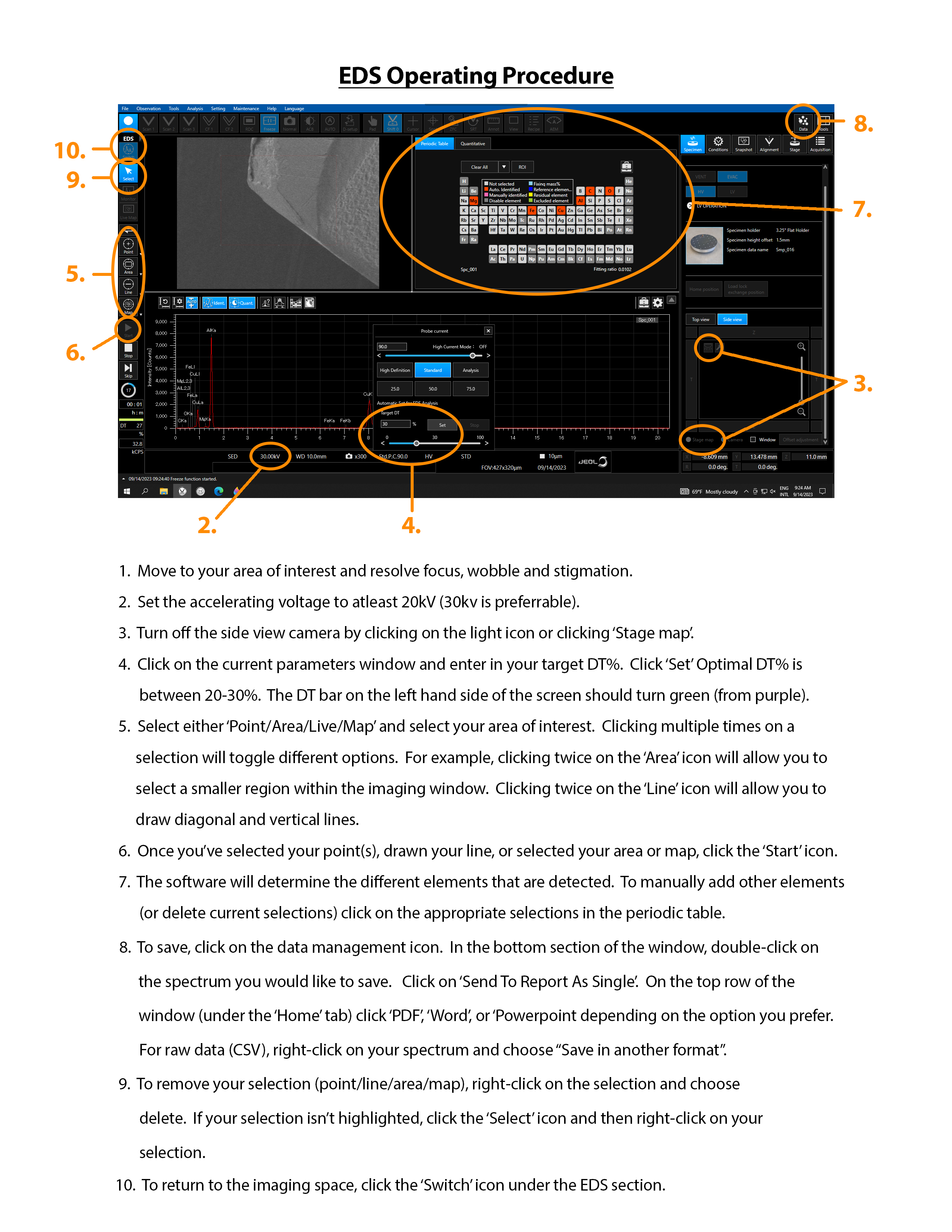
| + | *[https://wiki.nanofab.ucsb.edu/w/images/3/3a/EDS_SOP.jpg EDS Operating Procedure] |
||
| − | ===Imaging=== |
||
| − | |||
| − | *Resolution: |
||
| − | **1nm guaranteed at 15kV SEM mode |
||
| − | **2.5nm at 1kV in SEM mode |
||
| − | **1.5nm at 1kV in GB mode |
||
| − | *Magnification: |
||
| − | **SEM: x100 (at WD 25mm) to x1,000,000 (at WD 8mm) |
||
| − | **Low-Mag LM mode: x25 to x19,000 |
||
| − | *Imaging Modes/Detectors: |
||
| − | **SEI: secondary electron imaging |
||
| − | **LM: Low-magnification mode |
||
| − | **GB: Gentle-Beam mode |
||
| − | ***Applies negative voltage to sample stage to increase effective acceleration without increasing beam acceleration (reducing charging). |
||
| − | **LABE: Low-Angle Backscatter Electron detector |
||
| − | ***Inserts between the objective lens and the sample |
||
| − | ***Strong contrast between materials |
||
| − | **LEI: Lower Electron Detector |
||
| − | ***Detector is lower on chamber, creating strong topographical contrast. |
||
| − | *Accelerating Voltages: |
||
| − | **SEM: 0.5 to 30kV |
||
| − | **GB: 0.1 to 4.0kV |
||
| − | *Beam Currents: 10<sup>-13</sup> to 2x10<sup>-7</sup> A |
||
| − | |||
| − | ===Mechanical=== |
||
| − | |||
| − | *Max Sample Size: 4-inch wafer |
||
| − | *Stage movement: |
||
| − | **max: 70 x 50mm |
||
| − | **4-inch wafer: limited to ~25x25mm movement area from wafer center. |
||
| − | *Tilt: -5° to +70° |
||
| − | *Rotation: 360° |
||
| − | *Specimen holders : |
||
| − | **Copper and XYZ Carbon tape available |
||
| − | **4-inch wafer with topside clips |
||
| − | **1-inch holder for 30°/90°, 45°/90° mounting with tape or clips. |
||
| − | |||
| − | ==Operating Procedures== |
||
| − | {{Todo|upload procedures - printouts available at the tool}} |
||
Latest revision as of 21:08, 29 February 2024
| ||||||||||||||||||||||||||||||

About
The JEOL IT800HSL Field Emission Scanning Electron Microscope is used for imaging a variety of samples made in the facility.
Identical to SEM#1, but with EDAX module added.
Please see the SEM#1 page for main tool details & procedures.