Difference between revisions of "Dicing Saw (ADT)"
Jump to navigation
Jump to search
(Updated SOP) |
|||
| Line 28: | Line 28: | ||
==Operating Procedures== |
==Operating Procedures== |
||
| − | *[https://wiki.nanotech.ucsb.edu/w/images/8/ |
+ | *[https://wiki.nanotech.ucsb.edu/w/images/8/8c/ADT_SOP_Rev_G.pdf ADT Dicing Saw Standard Operating Procedure] |
*[https://wiki.nanotech.ucsb.edu/w/images/0/01/Tape_Station_SOP_Rev_A.pdf Tape Station Standard Operating Procedure] |
*[https://wiki.nanotech.ucsb.edu/w/images/0/01/Tape_Station_SOP_Rev_A.pdf Tape Station Standard Operating Procedure] |
||
*[[ADT 7100 - Recovering an Old Recipe (2019)|Recovering an Old Recipe]] |
*[[ADT 7100 - Recovering an Old Recipe (2019)|Recovering an Old Recipe]] |
||
Revision as of 12:30, 23 November 2022
| ||||||||||||||||||||||||||||||||
About
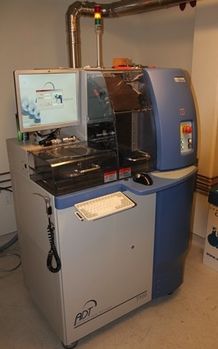
The ADT 7100 Dicing Saw is optimized for multi-angle dicing of thin, tight tolerance products up to 200 mm x 200 mm. It is currently setup for dicing up to 8” diameter wafers. Check the Dicing Saw Recipes page for the blades we currently stock.
An ADT WM-966 tape applicator & Ultron Systems UH104-8 UV lamp system is used to apply UV-release tape for securing die during dicing.
Contact the tool supervisor for blades and dicing frames for your group.
Detailed Specifications
- Maximum Wafer Size: 8"
- Parts mounted to UV-release tape for cutting
- Automated cut maps at multiple angles (0° and 90° typical)
- ~few micron alignment to on-wafer features.
- Thermocarbon Resnoid dicing blades provided by staff
Operating Procedures
- ADT Dicing Saw Standard Operating Procedure
- Tape Station Standard Operating Procedure
- Recovering an Old Recipe
Recipes
- Recipes > Packaging > Dicing Saw Recipes (ADT 7100)
Be sure to also see the recipes for protecting your sample from dicing dust, and mounting/unmounting.
