Calculators + Utilities
This page lists a few online calculators and utilities that are useful to lab users.
Fabrication Processes & Converters
- Thermal Oxide Calculator (BYU)
- Thermal Oxide Calculator (Leland Stanford Jr.)
- This Thermal Ox calculator allows you to tweak the calculation using the Partial Pressure variable, to match your experimental data.
- Conversion of Pressure Units (calculatoredge.com)
- Mean Free Path tables (Pfeiffer Vacuum)
- LelandStanfordJunior.com: Film Stress, Ion Implant, Thermal Oxidation, KOH Etching & online curve-fitting
Material Parameters
- WebElements: Compounds
- Boiling points of various compounds can tell you how volatile an etch product may be in a reactive ion etch, or whether they need to be wet-etched instead.
- Physical Properties of Semiconductors (Ioffe Institute)
- Kurt J Lesker: Material Deposition Chart
- Useful info about evaporating and sputtering many materials
- Kurt J. Lesker: Sputter Rates
- Sputter rates of various materials, indicative or hardness and dry etching properties.
Wet Etching
- Transene Inc. Chemical Compatibility Chart
- This table shows common metals and which Transene etchants they are attacked by/impervious to.
- A.R. Clawson, "Guide to references on III±V semiconductor chemical etching", 2001
- Enormous review of published wet etches of many semiconductors and alloys. The only thing it's missing is a hyperlinked table of contents.
Refractive Indices
Optical constants of many common materials. Useful for Optical thin-film analysis (ellipsometry/spectroscopic fitting), laser etch monitoring, optical filter/mirror/anti-reflection coating design, photonic devices etc.
Scripts + Programs
Analysis Programs
- AmScope Software - microscope image analysis software
- AmScope Calibration File containing calibrations for all NanoFab microscopes: Download Here
- Also available on Nanofiles-SFTP / Manuals / Amscope
- FIJI - scientific image anaylsis software
- The Microscope Measurement Tools plugin has pre-configured calibrations for NanoFab microscopes & SEMs, and allows you to draw length measurements.
- Calibrations in this plugin repository are out of date as of microscope upgrades in 2019.
- There are many other useful plugins, for particle counting, creating animations etc.
- The Microscope Measurement Tools plugin has pre-configured calibrations for NanoFab microscopes & SEMs, and allows you to draw length measurements.
- Gwyddion - free analysis software for Atomic Force Microscopes (AFMs) and other 3D data.
- Sophisticated leveling, slicing, roughness/particulate analysis functions etc.
- Can open Bruker NanoScope files, from the AFM
- ProfilmOnline.com (Filmetrics) - online analysis/storage/sharing of 3D topographical data and images.
- You can share an interactive 3D render of your AFM or Profilm3D scans with this tool.
- Example AFM Scan, taken with NanoFab equipment, shared online for interactive analysis (slice, flatten etc.).
CAD Layout Programs
Use these for designing your lithography mask plates.
L-Edit
Powerful multi-layer layout program. Sophisticated object instantiation and array layout, to reduce files sizes and easily push changes to multiple cells.
- UCSB's ECE dept. provides an academic license for this software (no industrial users!), email help@ece.ucsb.edu to obtain the software.
- Windows only.
- See this L-Edit Tutorial for a good starter guide. Written by Cherry Gupta, courtesy of Prof. Sumita Pennathur.
KLayout
A free, open-source, and fast/simple CAD tool for mask/reticle layout. Also has powerful functions, DRC, scriptiable and can handle very large files (GB's) efficiently. Download at klayout.de.
- Available on Windows, Mac or *Nix.
- Fast viewing of layer overlay, overlay multiple files, cell hierarchy, large (>1GB) files etc.
- Supports the same core functionality as L-Edit - hierarchical Cell Instances, arrays, programmable Cells (PCells) etc.
- Easily scriptable with Python or Ruby, with decent tutorials.
- KLayout Design Tips: important info on making "valid" CAD files, and setting up the program for efficient use.
- Univ. of Waterloo QNFCF produced some good video tutorials on KLayout, here.
AutoCAD
Although AutoCAD can produce a valid DXF file, we see many design/conversion issues with these files. This is because many shapes and line-types (Line/polyline/LWLine for example) used in AutoCAD don't convert as expected into the polygons needed for printing. Also the DXF file format itself often creates problems, such as incorrect scaling or badly-filled/unclosed polygons.
CAD Design Tips
Cells and Instancing
All major chip layout programs support "Cells" and similar structures for hierarchical layout. It is highly recommended that you understand and use the concept of "Cells" in your design. This circumvents many problems with enormous file sizes (due to huge numbers of identical polygons), and if used properly, helps tremendously with programming the Stepper lithography machines. Links to documentation below:
- Create a new cell, and instancing that cell: KLayout Docs : Creating a Cell instance
- Viewing only some levels of the heirachy, to prevent drawing all objects: KLayout Docs: Viewing Cell Heirarchy
File Types
OASIS files tend to be much smaller than GDS files, and they also save the Layer Names (not just number). Alternatively, in KLayout the function File > Save Session will save the entire view including layer styles and window/zoom locations will be saved. You can share this file, as the entire design file is embedded within it, but it may not be as robust between KLayout versions.
DXF Files can often cause problems because the format varies widely depending on the program they are exported from. For example, DXF can lose the "scaling" causing polygons to be 1000x larger than expected, or unexpectedly cause some shares to get filled in.
KLayout Design Tips
See the above page for important info on making "valid" CAD files, and setting up KLayout for efficient use.
Handling very large files
If you will be generating millions of identical shapes (eg. repeating array of circles), the file size can quickly become enormous due to all the stored polygon points. You can reduce the number of polygon points stored by:
- Reduce the number of points in each shape/circle if possible.
- Use Cell instancing so that only one, or a few, polygons are defined, and that same polygon is then only referenced as a repeating Cell instance. (See above for tutorials).
- The OAS file type generates much smaller files, and most photomask vendors can accept this. Photomask vendors are used to handling large files.
- Photomask vendors are able to take multiple files and insert them into the final reticle – you just need to provide a clear schematic showing the exact insertion coordinates for each file (with respect to the origin of each file). They can also do some boolean operations (for a fee).
Example CAD File
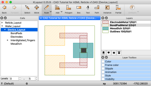
Here is an example CAD file, showing the use of Layers and Cells, designed in KLayout. The device is fictional, for illustrative purposes only.
- CAD_Tutorial_for_ASML_Reticle_v1.OAS , or GDS version (Demis D. John)
- Cell "Device_Layout" shows a single device, with each Layer overlaid as it would be in a fabricated device. Each Layer (eg. a "process step" such as Mesa etch, Pad Metal etc.) is placed into it's own Cell.
- Every Cell's Origin (0,0) lies on top of one another in the final Device_Layout.
- One way this can be accomplished is by selecting the objects/polygons you want to make into a new Cell, then use the function Edit > Selection > Make Cell, and uncheck the "Put Origin at..." checkbox, so the new Cell maintains the same origin as the original view.
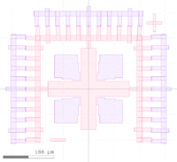
- The Cell "Reticle_Layout" can be exported by itself (right-click the Cell name), for sending to the photomask manufacturer.
- Here is an example GDS file (download) for submission to the photomask manufacturer, with all objects moved to a single Layer.
- See the ASML Mask Making Guidelines page for an example of how to program this Reticle into an ASML Stepper job.
CAD Files & Templates
General CAD files for Litho
- Vented Font (GDS) - a font good for liftoff (no enclosed holes). (Designed by Demis D. John)
- See this comment for instructions on installing the font into KLayout.
- Alignment/Registration Vernier Scales (GDS) - used to measure the misalignment between different layers (step=0.1um). (Designed by Demis D. John)
- Resolution Test structures - To Be Added
- Contact Alignment Mark:
- CNF Contact Marks - designed by the Cornell Nanoscale Science & Technology Facility staff.
- "Polygons are Clear" polarity, so 2nd layer has transparent region around alignment mark.
- Male/female alignment marks with vernier (step=0.5um): OASIS / GDS format (Designed by Demis D. John)
- 2nd layer has cells with both polarities
- CNF Contact Marks - designed by the Cornell Nanoscale Science & Technology Facility staff.
GCA Stepper
- GCA Photomask Template: Dark-field (polygons/objects are clear) at 5x Magnification (GDS)
- This template is designed to be submitted to the photomask vendor to print as-is, no scaling applied.
- Insert your designs into the template as Instances scaled UP by 5x.
- During exposure, set the blades to 90/90 to block out AutoStep200 DFAS openings
- GCA Global Alignment Mark CAD File (GDS)
- GCA Local Alignment Mark (GDS)
- GCA Local Alignment Mark Dotted (GDS) - helps for low-contrast topography
ASML Stepper
- ASML On-Wafer Alignment Mark (GDS) - see more info on the ASML Stepper#3 page.
- Example Reticle/Mask CAD File, designed in KLayout.
Heidelberg MLA150
Other sources of lithography CAD files
- MEMS Exchange - has some useful alignment markers, registration/alignment verniers etc.
- EPFL CMi - CMi layout template has some useful guidelines and resolution test structures.
General Calculators
- Anaconda Python
- A free Matlab-like IDE and GUI, using the Python language. The Spyder interface is modeled after Matlab.
- Includes the scientific Python libraries needed for array math (numpy), plotting (matplotlib), data science (pandas) and many others. Many open-source packages are available to extend capabilities. The PyVisa module adds equipment control capabilities for automated measurements.
- Octave Online Interpreter (online-utility.org)
- A Matlab-like command-line interface, powered by Python Octave.
- Wolfram Alpha
- A versatile online interpreter/calculator, allowing calculations such as "Volume of 1.5g of Silicon", "melting point of SiO2" or "520°C in Fahrenheit".
Python Scripts
These scripts are best run in the Spyder IDE, which is easily installed via Anaconda, Python(X,Y).
If you use/modify these scripts in a publication, please consider citing the author(s). See our publication policy for more info.
Keithley I-V Sweep
- Sweep voltage and plot current vs. voltage using a Keithley SMU.
- Already installed at the Probe Station in Bay 4, and on the QFI Thermal Microscope (Use Spyder (Anaconda Python) to run).
- Requires the pyvisa python module.
QFIScope Thermal Analysis (Demis D. John)
- Import 2D temperature data from the IR Thermal Microscope (QFI) and plot temperature profiles at user-specified locations.
- Already installed on the QFI Infrared Microscope.
Laser Etch Monitor Simulation in Python (Demis D. John)
- Simulate your laser endpoint signal as you dry-etch through a stack of thin-film layers, using an open-source electromagnetics module.
Optical Constants of Nanofab Films - nk.py (Demis D. John)
- Python functions for returning n (refractive index) & k (extinction coefficient) of various NanoFab thin-films at a specified wavelength (aka. optical dispersion models)


