CDE ResMap Quick-Start instructions
Jump to navigation
Jump to search
- Depending on the program you run, your sample location may be different.
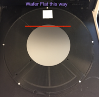
- In general, programs for full 4-inch wafers require the wafer to be centered on the stage.
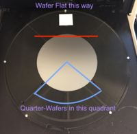
- Wafer flat should face the white sticker on the stage.
- Programs for Quarter wafers will measure opposite the white stick. See image below.
- You can always load a 6" wafer (eg. from teh discarded ICP carriers) and run a program to see where it is going to measure.
Quick Measurement Procedure
- Select Operator > Run Recipe
- Choose a recipe in "UCSB Users"
- Filename indicates whether it will measure a Full or quarter wafer, number of points, wafer diameter etc.
- Choose a "Filename" for your data. Enable "Auto Plot" to show a contour plot.
- [Run] to perform the scan.
- You can Abort the scan by pressing Any key, and click [Abort] at the top.
- Sheet resistance of every measured point is shown on the next screen.
- "Rs" is sheet resistance, "RsAvg" is Average of all measured points.

