Difference between revisions of "Atomic Layer Deposition (Oxford FlexAL)"
(added cluster config section) |
m (typo/grammar) |
||
| Line 18: | Line 18: | ||
The system is load-locked and can accommodate sample temperatures up to 550°C. Processing temperature windows are defined for each material based on growth limitations. The system is step-by-step programmable through a flexible GUI interface. In-situ ellipsometry between growth cycles and mass spectrometry during growth are both available. |
The system is load-locked and can accommodate sample temperatures up to 550°C. Processing temperature windows are defined for each material based on growth limitations. The system is step-by-step programmable through a flexible GUI interface. In-situ ellipsometry between growth cycles and mass spectrometry during growth are both available. |
||
| − | === |
+ | ===Cluster Configuration=== |
| − | We have three separate chambers on the Oxford Cluster tool, two of which are ALD chambers. |
+ | We have three separate chambers on the Oxford Cluster tool, two of which are ALD chambers. |
| + | One ALD chamber is dedicated to metals and the other dedicated to dielectrics. The other chamber on the cluster is the [[CAIBE (Oxford Ion Mill)|Oxford Ion Mill]]. |
||
| − | The two chambers on the Oxford Cluster tool are separated by film type: |
||
*Chamber #1: ALD Dielectrics Films only |
*Chamber #1: ALD Dielectrics Films only |
||
Revision as of 14:13, 26 November 2019
| |||||||||||||||||||||
About
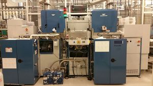
The Oxford Instruments FlexAL Atomic Layer Deposition system at UCSB is a plasma-enhanced ALD system for the precise growth of ultra-thin oxides and nitrides. Self-limiting layer by layer growth ensures precise control, film conformality, and repeatability of the films.
The system currently has metallorganic precursors for Aluminum, Hafnium, Titanium, Platinum, Zirconium, and Silicon oxides and nitrides. Water and Ozone are available for thermal oxides and Oxygen, Ammonia, Nitrogen, and Hydrogen are available for plasma assisted oxides and nitrides. Remote ICP plasma powers up to 600W are possible.
The system is load-locked and can accommodate sample temperatures up to 550°C. Processing temperature windows are defined for each material based on growth limitations. The system is step-by-step programmable through a flexible GUI interface. In-situ ellipsometry between growth cycles and mass spectrometry during growth are both available.
Cluster Configuration
We have three separate chambers on the Oxford Cluster tool, two of which are ALD chambers.
One ALD chamber is dedicated to metals and the other dedicated to dielectrics. The other chamber on the cluster is the Oxford Ion Mill.
- Chamber #1: ALD Dielectrics Films only
- Chamber #2: Oxford Ion Mill
- Chamber #3: ALD Metal Films only
Procedures & Documentation
- Operating Instructions
- Includes recipe names for various films, and approx. dep. rates
- Film Thicknesses are restricted to 30nm or less.
- Thicker films are allowed with prior staff approval - please ask Bill Mitchell if you want to deposit a thicker film!
ALD Recipes
- See the Atomic Layer Deposition: Recipes page for recipes and thin-film data/measurements.
- Only staff-provided recipes are allowed to be run on this tool, as achieving the atomic-layer regime is rather complex. Bill Mitchell is the resident expert on ALD recipe development.
