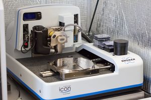
Atomic Force Microscope (Bruker ICON)
|
About
The Dimension 3100 Nanoman AFM from Veeco provides a variety of high resolution surface imaging techniques and the ability to manipulate or create nanoscale structures directly. Techniques available for imaging include contact mode AFM, tapping mode AFM, Scanning Tunnelling AFM, Conductive AFM, and Scanning Capacitance Microscopy. With the Nanoman option, the X and Y deflecting piezo-elements are independently controlled, allowing for precise and direct placement of the tip anywhere within the field. Direct manipulation of particles on the surface is then possible by dragging the tip in the desired direction. This feedback control, coupled with direct control of conductive tip and substrate voltages, allows for direct-write oxidation on a variety of surfaces to create or modify nanostructures through local anodization.
Detailed Specifications
- Conductive AFM modules for nA-microAmp current measurements
- Tunneling AFM modulefor pA-nA current measurements
- Scanning Capacitance Microscopy
- Resolution: Sub-nm height-measurement capability; X-Y resolution tip dependent
- Registration tolerance to a known mark: Field size dependent
- Minimum substrate size: small pieces
- Largest substrate size: 100 mm wafer
- Oxidation Line widths: Call for info.
