ASML Stepper 3 Dicing Guide Programming
Jump to navigation
Jump to search
The printable version is no longer supported and may have rendering errors. Please update your browser bookmarks and please use the default browser print function instead.
How to program the ASML DUV Stepper #3 to place dicing guides in between die.
UPDATE: doesn’t work: Ning tried this and found these patterns were too difficult to see on the disconfirm saw. Demis: new method, use ASML’s Alignment Mark distribution function to use SPM-X/Y marks as dicing guides. Carefully not to distribute too many - there is a software limit on number of exposures per Image.
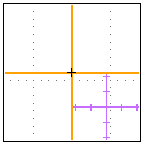
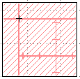
- Determine a lithography step in the fabrication process during which the addition of dicing guides (crosses) would be acceptable and visible during dicing. There are both positive and negative versions of the Cross pattern.
- When programming the job, add an new Image in
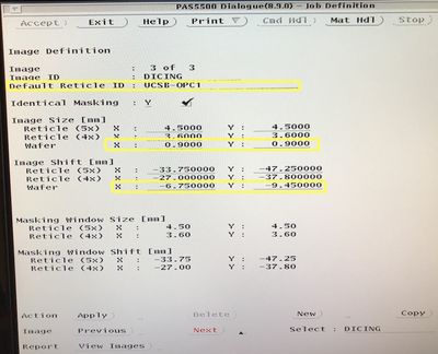
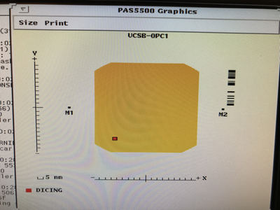
Wafer Layout > Image Definitionfor the DicingGuides image, as so:- Reticle ID: "UCSB-OPC1" (hyphenated)
- For Positive PR image:
- Image Size (Wafer): X = 0.90000; Y = 0.90000 mm
- Image Shift (Wafer): X = -6.750000; Y= -9.450000 mm
- For Negative PR Image:
- Image Size (wafer scale): X = 0.710000 ; Y = 0.710000 mm
- Image Shift (wafer scale): X = 6.750000 ; Y = -9.450000 mm
- More info on either pattern can be found here.
- Under
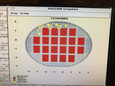
Wafer Layout > Image Distribution, add anImage-to-Cell Shiftof half the die X/Y size, andApplyto all die, to place the marks at the corner of every die.- The software will only let you place the die at the upper-right (+X,+Y) corner. To include the lower-left corners, you will need to make sure you enabled the
Wafer Layout > Cell Structure > Die Definition > # of Dies & Minimum per Celloptions too shoot partial die at the wafer edges. - Make sure they don't expose over any of your other alignment marks!
- The software will only let you place the die at the upper-right (+X,+Y) corner. To include the lower-left corners, you will need to make sure you enabled the
