Difference between revisions of "ASML Stepper 3 - UCSB Test Reticles"
m (→Alignment Markers: note polarity) |
m (→Alignment Markers: MA6 mark: contact Brian/Demis for GDS) |
||
| Line 57: | Line 57: | ||
Note the Polarity - will ''expose'' a ~550µm area. |
Note the Polarity - will ''expose'' a ~550µm area. |
||
| + | |||
| + | Contact [[Demis D. John|Demis]] or [[Brian Thibeault|Brian]] for the CAD file for the male/female version of this mark. |
||
|White is Chrome, Striped area is Clear |
|White is Chrome, Striped area is Clear |
||
[[File:Align Front - Screen Shot 2018-07-23 at 11.32.16 AM.png|frameless|146x146px]] |
[[File:Align Front - Screen Shot 2018-07-23 at 11.32.16 AM.png|frameless|146x146px]] |
||
Revision as of 13:50, 4 June 2019
Reticle ID: "UCSB-OPC1"
This reticle is always installed in the system, in the "System Reticles" Box #1.
The reticle contains alignment markers for various NanoFab lithography systems, along with resolution test structures and patterns for calibrating optical proximity correction on the system. Some patterns are proprietary to the mask designer, so we can not share the full GDS CAD file.
Alignment Markers
| Image ID | Image Size
X , Y (Wafer, mm) |
Image Shift
X , Y (Wafer, mm) |
Notes/Description | Schematics |
|---|---|---|---|---|
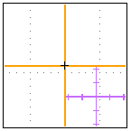
| GCA_Align | 0.530000 , 0.140000 | -6.750000 , 9.450000 | ImageShift references the center of the -X- "global" mark.
The ==||| "Local" mark is X+200µm to the right has 1.1mm margin on all sides |
White is Chrome, Pattern is Clear
|
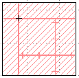
| E-Beam Litho Alignment Mark - Positive | 0.900000 , 0.900000 | -6.750000 , -9.450000 | ImageShift is the center coords of the larger "+" mark
Smaller "+" mark is (0.225,-0.225)mm down-right 0.925mm margin on all sides |
White is Chrome, Pattern is Clear |
| E-Beam Litho Alignment Mark - Negative | 0.710000 , 0.710000 | 6.750000 , -9.450000 | ImageShift is the center coords of the larger "+" mark
Smaller "+" mark is (0.225,-0.225)mm down-right Blank (masked) space on left+top sides 1.0mm margin on all sides |
Striped area is Clear |
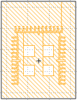
| Contact_Mark | 0.564000 , 0.564000 | 6.750000 , 9.450000 | ImageShift references the center of the contact alignment mark "+"
with 1.1mm margin on all sides Note the Polarity - will expose a ~550µm area. Contact Demis or Brian for the CAD file for the male/female version of this mark. |
White is Chrome, Striped area is Clear |
Resolution Test Charts
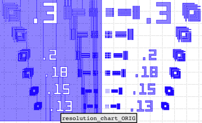
The Resolution test charts are repeated all across the reticle, in order to test for lens aberrations. You can have the system expose only a single resolution chart, but since they are placed closely together on the reticle, it's very likely that partial shots of adjacent charts will also be exposed.
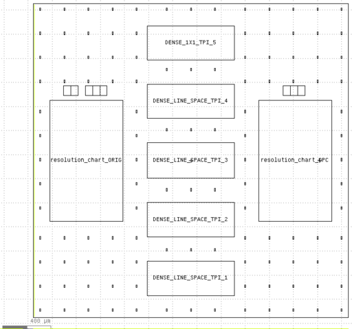
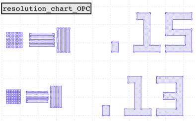
In addition, the repeating cells allow us to test for the proper optical proximity correction (OPC) algorithm. The Five Dense_... patterns are for calibrating the OPC algorithm, and are not for user analysis.
Calibration Chart Layout
Cell name is "UCSB_Cal", with coordinates below pointing to center of this cell.
Resolution Chart Schematic
"resolution_chart_ORIG" cell in the above.
The ""resolution_chart_OPC" version has an optical proximity correction algorithm applied:
Coords for "resolution_chart" Calibration patterns
Image coords for each of the "resolution_chart_ORIG" cells. You can pick just one of these for shooting a resolution test structure. The purpose of the many different locations is to check for variations due to lens aberrations. You could just choose one near the center of the plate to test your process, or you could choose a chart that is in a similar location as the pattern you're shooting on your mask plate.
Note that some portion of the adjacent patterns will likely be exposed as well, due to the patterns not being surrounded by 1mm of chrome. Make sure you set your Cell Size large enough to make sure the bleed-over doesn't overlap with adjacent die.
| Image Size
X , Y (Wafer, mm) |
Image Shift
X (Wafer, mm) |
Image Shift
Y (Wafer, mm) |
|---|---|---|
| 0.605 , 1.005 | -10.115000 | 12.150000 |
| same for each | -7.415000 | 12.150000 |
| " " | -4.715000 | 12.150000 |
| " " | -2.015000 | 12.150000 |
| " " | 0.685000 | 12.150000 |
| " " | 3.385000 | 12.150000 |
| " " | 6.085000 | 12.150000 |
| " " | 8.785000 | 12.150000 |
| -10.115000 | 9.450000 | |
| Alignment Marker | ||
| -4.715000 | 9.450000 | |
| -2.015000 | 9.450000 | |
| 0.685000 | 9.450000 | |
| 3.385000 | 9.450000 | |
| Alignment Marker | ||
| 8.785000 | 9.450000 | |
| -10.115000 | 6.750000 | |
| -7.415000 | 6.750000 | |
| -4.715000 | 6.750000 | |
| -2.015000 | 6.750000 | |
| 0.685000 | 6.750000 | |
| 3.385000 | 6.750000 | |
| 6.085000 | 6.750000 | |
| 8.785000 | 6.750000 | |
| -10.115000 | 4.050000 | |
| -7.415000 | 4.050000 | |
| -4.715000 | 4.050000 | |
| -2.015000 | 4.050000 | |
| 0.685000 | 4.050000 | |
| 3.385000 | 4.050000 | |
| 6.085000 | 4.050000 | |
| 8.785000 | 4.050000 | |
| -10.115000 | 1.350000 | |
| -7.415000 | 1.350000 | |
| -4.715000 | 1.350000 | |
| -2.015000 | 1.350000 | |
| 0.685000 | 1.350000 | |
| 3.385000 | 1.350000 | |
| 6.085000 | 1.350000 | |
| 8.785000 | 1.350000 | |
| -10.115000 | -1.350000 | |
| -7.415000 | -1.350000 | |
| -4.715000 | -1.350000 | |
| -2.015000 | -1.350000 | |
| 0.685000 | -1.350000 | |
| 3.385000 | -1.350000 | |
| 6.085000 | -1.350000 | |
| 8.785000 | -1.350000 | |
| -10.115000 | -4.050000 | |
| -7.415000 | -4.050000 | |
| -4.715000 | -4.050000 | |
| -2.015000 | -4.050000 | |
| 0.685000 | -4.050000 | |
| 3.385000 | -4.050000 | |
| 6.085000 | -4.050000 | |
| 8.785000 | -4.050000 | |
| -10.115000 | -6.750000 | |
| -7.415000 | -6.750000 | |
| -4.715000 | -6.750000 | |
| -2.015000 | -6.750000 | |
| 0.685000 | -6.750000 | |
| 3.385000 | -6.750000 | |
| 6.085000 | -6.750000 | |
| 8.785000 | -6.750000 | |
| -10.115000 | -9.450000 | |
| Alignment Marker | ||
| -4.715000 | -9.450000 | |
| -2.015000 | -9.450000 | |
| 0.685000 | -9.450000 | |
| 3.385000 | -9.450000 | |
| Alignment Marker | ||
| 8.785000 | -9.450000 | |
| -10.115000 | -12.150000 | |
| -7.415000 | -12.150000 | |
| -4.715000 | -12.150000 | |
| -2.015000 | -12.150000 | |
| 0.685000 | -12.150000 | |
| 3.385000 | -12.150000 | |
| 6.085000 | -12.150000 | |
| 8.785000 | -12.150000 | |
Coords for "UCSB_Cal" Calibration Patterns
Each of the above "UCSB_Cal" cells, including all 7 patterns, is repeated on the following coordinates across the plate (coords are to the center of the "UCSB_Cal" cell):
| Image Size
X , Y (Wafer, mm) |
Image Shift
X (Wafer, mm) |
Image Shift
Y (Wafer, mm) |
|---|---|---|
| 2.610000 , 2.610000 | -9.450000 | 12.150000 |
| same as above | -6.750000 | 12.150000 |
| " " | -4.050000 | 12.150000 |
| " " | -1.350000 | 12.150000 |
| " " | 1.350000 | 12.150000 |
| " " | 4.050000 | 12.150000 |
| " " | 6.750000 | 12.150000 |
| " " | 9.450000 | 12.150000 |
| -9.450000 | 9.450000 | |
| Alignment Marker | ||
| -4.050000 | 9.450000 | |
| -1.350000 | 9.450000 | |
| 1.350000 | 9.450000 | |
| 4.050000 | 9.450000 | |
| Alignment Marker | ||
| 9.450000 | 9.450000 | |
| -9.450000 | 6.750000 | |
| -6.750000 | 6.750000 | |
| -4.050000 | 6.750000 | |
| -1.350000 | 6.750000 | |
| 1.350000 | 6.750000 | |
| 4.050000 | 6.750000 | |
| 6.750000 | 6.750000 | |
| 9.450000 | 6.750000 | |
| -9.450000 | 4.050000 | |
| -6.750000 | 4.050000 | |
| -4.050000 | 4.050000 | |
| -1.350000 | 4.050000 | |
| 1.350000 | 4.050000 | |
| 4.050000 | 4.050000 | |
| 6.750000 | 4.050000 | |
| 9.450000 | 4.050000 | |
| -9.450000 | 1.350000 | |
| -6.750000 | 1.350000 | |
| -4.050000 | 1.350000 | |
| -1.350000 | 1.350000 | |
| 1.350000 | 1.350000 | |
| 4.050000 | 1.350000 | |
| 6.750000 | 1.350000 | |
| 9.450000 | 1.350000 | |
| -9.450000 | -1.350000 | |
| -6.750000 | -1.350000 | |
| -4.050000 | -1.350000 | |
| -1.350000 | -1.350000 | |
| 1.350000 | -1.350000 | |
| 4.050000 | -1.350000 | |
| 6.750000 | -1.350000 | |
| 9.450000 | -1.350000 | |
| -9.450000 | -4.050000 | |
| -6.750000 | -4.050000 | |
| -4.050000 | -4.050000 | |
| -1.350000 | -4.050000 | |
| 1.350000 | -4.050000 | |
| 4.050000 | -4.050000 | |
| 6.750000 | -4.050000 | |
| 9.450000 | -4.050000 | |
| -9.450000 | -6.750000 | |
| -6.750000 | -6.750000 | |
| -4.050000 | -6.750000 | |
| -1.350000 | -6.750000 | |
| 1.350000 | -6.750000 | |
| 4.050000 | -6.750000 | |
| 6.750000 | -6.750000 | |
| 9.450000 | -6.750000 | |
| -9.450000 | -9.450000 | |
| Alignment Marker | ||
| -4.050000 | -9.450000 | |
| -1.350000 | -9.450000 | |
| 1.350000 | -9.450000 | |
| 4.050000 | -9.450000 | |
| Alignment Marker | ||
| 9.450000 | -9.450000 | |
| -9.450000 | -12.150000 | |
| -6.750000 | -12.150000 | |
| -4.050000 | -12.150000 | |
| -1.350000 | -12.150000 | |
| 1.350000 | -12.150000 | |
| 4.050000 | -12.150000 | |
| 6.750000 | -12.150000 | |
| 9.450000 | -12.150000 | |
