ASML 5500 Mask Making Guidelines
Jump to navigation
Jump to search
- Use commercial mask/reticle houses: Photronics, Toppan, Compugraphics, etc. Instruct vendor that this will be used on an ASML 5500/300 system. They have all outer templates to make your mask match our system. You just provide them the data you want printed at wafer scale (1X) and they'll insert it into the template.
- Toppan Order Form via Digidat
- Academic users may use the UCSB-specific Toppan quote for pricing. Industrial users will have to get their own pricing.
- Email Brian Thibeault or Demis D. John for info.
- Reduction is 4X, mask makers will scale data to 4X size, which will determine price. Scale your mask critical dimensions (CD) and tolerances accordingly.
- Masks must be Quartz, 6" x 6" x 0.25” thick.
- Layer-to-layer alignment marks are provided by a calibration mask in our system. No need to put alignment marks on your CAD file.
- Spacing between mask-plate fields : 1mm of Chrome between fields (at wafer scale) in order for the reticle masking blades to blank off unwanted areas.
- Field Sizes Available (Wafer Scale, 1x):
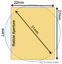
- The full field useable exposure area is limited to the intersection of a 31mm diameter circle and a rectangle of dimensions 22mm x 27mm. See the schematic below for an illustration.
- For High Resolution 0.63 NA: 21mm in X, 21mm in Y
- For 0.4 to 0.57 NA: 22mm in X, 22mm in Y
- Other rectangular sizes available, that fit within the lens/aperture intersection:
- 21mm x 23mm (X width x Y height)
- 20mm x 24mm
- 19mm x 25mm
- 18mm x 25.5mm
- 17mm x 26mm
- 16mm x 26.5mm
- 15mm x 27mm
- In general, 250nm resolution will resolve over the entire field. Anything smaller than this may not resolve closer to the edges of the field where lens quality degrades, and will also have a smaller viable process window (tolerance of exposure/bake/develop parameters). A number of users have shot ~150nm features.
Templates
- When programming your job at the tool, you can fill out this Spreadsheet using your CAD file before starting your job programming:
