Difference between revisions of "ASML 5500 Mask Making Guidelines"
Jump to navigation
Jump to search
(copied Mask Making Guidelines PDF & inserted illumination field schematic) |
m (moved image on page) |
||
| Line 2: | Line 2: | ||
# Reduction is 4X in ASML, mask makers will scale data to 4X size, which will determine price. Scale your mask critical dimensions and tolerances accordingly. |
# Reduction is 4X in ASML, mask makers will scale data to 4X size, which will determine price. Scale your mask critical dimensions and tolerances accordingly. |
||
# Masks must be Quartz, should be 0.25” thick. |
# Masks must be Quartz, should be 0.25” thick. |
||
| − | # Layer-to-layer alignment marks are provided by a calibration mask in our system. No need to put alignment marks on your mask. |
+ | # Layer-to-layer alignment marks are provided by a calibration mask in our system. No need to put alignment marks on your mask. |
# Field Sizes Available (Wafer Scale, 1x): |
# Field Sizes Available (Wafer Scale, 1x): |
||
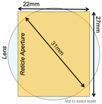
## The full field useable exposure area is limited to the intersection of a 31mm diameter circle and a rectangle of dimensions 22mm x 27mm. See the schematic below for an illustration. |
## The full field useable exposure area is limited to the intersection of a 31mm diameter circle and a rectangle of dimensions 22mm x 27mm. See the schematic below for an illustration. |
||
## For High Resolution 0.63 NA: 21mm in X, 21mm in Y |
## For High Resolution 0.63 NA: 21mm in X, 21mm in Y |
||
## For 0.4 to 0.57 NA: 22mm in X, 22mm in Y |
## For 0.4 to 0.57 NA: 22mm in X, 22mm in Y |
||
| + | ##[[File:ASML Stepper 3 - Field Sizes - Screen Shot 2018-02-21 at 1.40.22 PM.png|alt= Schematic of lens/aperture illumination|border|right|204x204px|Schematic of lens/aperture illumination. Fit a rectangle within this field to get the rectangular field sizes above.]] |
||
## Other rectangular sizes available, that fit within the lens/aperture intersection: |
## Other rectangular sizes available, that fit within the lens/aperture intersection: |
||
### 21mm x 23mm |
### 21mm x 23mm |
||
Revision as of 15:07, 21 February 2018
- Use professional mask/reticle houses: Photronics, Toppan, Compugraphics, etc. Instruct vendor that this will be used on an ASML 5500/300 system. They have all outer templates for the mask that match our system. You just provide them the data you want printed at wafer scale (1X).
- Reduction is 4X in ASML, mask makers will scale data to 4X size, which will determine price. Scale your mask critical dimensions and tolerances accordingly.
- Masks must be Quartz, should be 0.25” thick.
- Layer-to-layer alignment marks are provided by a calibration mask in our system. No need to put alignment marks on your mask.
- Field Sizes Available (Wafer Scale, 1x):
- The full field useable exposure area is limited to the intersection of a 31mm diameter circle and a rectangle of dimensions 22mm x 27mm. See the schematic below for an illustration.
- For High Resolution 0.63 NA: 21mm in X, 21mm in Y
- For 0.4 to 0.57 NA: 22mm in X, 22mm in Y
- Other rectangular sizes available, that fit within the lens/aperture intersection:
- 21mm x 23mm
- 20mm x 24mm
- 19mm x 25mm
- 18mm x 25.5mm
- 17mm x 26mm
- 16mm x 26.5mm
- 15mm x 27mm
- In general, 250nm resolution will resolve over the entire field. Anything smaller than this may not resolve closer the edges of the field where lens quality degrades, and will also have a smaller viable process window (tolerance of exposure/bake/develop parameters).
- Spacing between fields : 1mm of Chrome between fields (at wafer scale) in order to blank off unwanted areas.
